LTC3555/LTC3555-X
28
3555fe
For more information www.linear.com/LTC3555
Alternate NTC Thermistors and Biasing
The LTC3555 family provides temperature qualified charg-
ing if a grounded thermistor and a bias resistor are con-
nected to NTC. By using a bias resistor whose value is equal
to the room temperature resistance of the thermistor (R25)
the upper and lower temperatures are pre-programmed
to approximately 40°C and 0°C, respectively (assuming
a Vishay “Curve 1” thermistor).
The upper and lower temperature thresholds can be ad-
justed by either a modification of the bias resistor value
or by adding a second adjustment resistor to the circuit.
If only the bias resistor is adjusted, then either the upper
or the lower threshold can be modified but not both. The
other trip point will be determined by the characteristics
of the thermistor. Using the bias resistor in addition to an
adjustment resistor, both the upper and the lower tempera-
ture trip points can be independently programmed with
the constraint that the difference between the upper and
lower temperature thresholds cannot decrease. Examples
of each technique are given below.
NTC thermistors have temperature characteristics which
are indicated on resistance-temperature conversion tables.
The Vishay-Dale thermistor NTHS0603N011-N1002F, used
in the following examples, has a nominal value of 10k
and follows the Vishay Curve 1 resistance-temperature
characteristic.
In the explanation below, the following notation is used.
R25 = Value of the Thermistor at 25°C
R
NTC|COLD
= Value of thermistor at the cold trip point
R
NTC|HOT
= Value of the thermistor at the hot trip point
α
COLD
= Ratio of R
NTC|COLD
to R25
α
HOT
= Ratio of R
NTC|HOT
to R25
R
NOM
= Primary thermistor bias resistor (see Figure 5a)
R1 = Optional temperature range adjustment resistor
(see Figure 5b)
The trip points for the LTC3555 familys temperature
qualification are internally programmed at 0.349 V
BUS
for
the hot threshold and 0.765 V
BUS
for the cold threshold.
Therefore, the hot trip point is set when:
R
NTC|HOT
R
NOM
+R
NTC|HOT
V
BUS
= 0.349 V
BUS
and the cold trip point is set when:
R
NTC|COLD
R
NOM
+R
NTC|COLD
V
BUS
= 0.765 V
BUS
Solving these equations for R
NTC|COLD
and R
NTC|HOT
results in the following:
R
NTC|HOT
= 0.536 R
NOM
and
R
NTC|COLD
= 3.25 R
NOM
APPLICATIONS INFORMATION
Figure 5. NTC Circuits
(5a)
(5b)
+
+
R
NOM
10k
R
NTC
10k
NTC
0.1V
NTC_ENABLE
3555 F05a
LTC3555/LTC3555-X
NTC BLOCK
TOO_COLD
TOO_HOT
0.765 • V
BUS
0.349 • V
BUS
+
3
V
BUS
V
BUS
T
+
+
R
NOM
10.5k
R
NTC
10k
R1
1.27k
NTC
V
BUS
V
BUS
0.1V
NTC_ENABLE
3555 F05b
TOO_COLD
TOO_HOT
0.765 • V
BUS
0.349 • V
BUS
+
3
LTC3555/LTC3555-X
NTC BLOCK
T
LTC3555/LTC3555-X
29
3555fe
For more information www.linear.com/LTC3555
By setting R
NOM
equal to R25, the above equations result
in α
HOT
= 0.536 and α
COLD
= 3.25. Referencing these ratios
to the Vishay Resistance-Temperature Curve 1 chart gives
a hot trip point of about 40°C and a cold trip point of about
0°C. The difference between the hot and cold trip points
is approximately 40°C.
By using a bias resistor, R
NOM
, different in value from R25,
the hot and cold trip points can be moved in either direction.
The temperature span will change somewhat due to the non-
linear behavior of the thermistor. The following equations can
be used to easily calculate a new value for the bias resistor:
R
NOM
=
α
HOT
0.536
R25
R
NOM
=
α
COLD
3.25
R25
where α
HOT
and α
COLD
are the resistance ratios at the
desired
hot and cold trip points. Note that these equations
are linked. Therefore, only one of the two trip points can
be chosen, the other is determined by the default ratios
designed in the IC. Consider an example where a 60°C
hot trip point is desired.
From the Vishay Curve 1 R-T characteristics, α
HOT
is 0.2488
at 60°C. Using the above equation, R
NOM
should be set to
4.64k. With this value of R
NOM
, the cold trip point is about
16°C. Notice that the span is now 44°C rather than the
previous 40°C. This is due to the decrease in “temperature
gain” of the thermistor as absolute temperature increases.
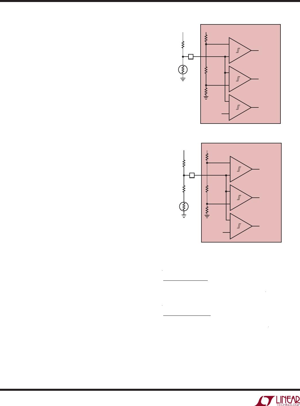
The upper and lower temperature trip points can be inde-
pendently programmed by using an additional bias resistor
as shown in Figure 5b. The following formulas can be used
to compute the values of R
NOM
and R1:
R
NOM
=
α
COLD
α
HOT
2.714
R25
R1= 0.536 R
NOM
α
HOT
R25
For example, to set the trip points to 0°C and 45°C with
a Vishay Curve 1 thermistor choose:
R
NOM
=
3.266 0.4368
2.714
10k = 10.42k
the nearest 1% value is 10.5k:
R1 = 0.536 10.5k – 0.4368 10k = 1.26k
the nearest 1% value is 1.27k. The final circuit is shown
in Figure 5b and results in an upper trip point of 45°C and
a lower trip point of 0°C.
USB Inrush Limiting
When a USB cable is plugged into a portable product,
the inductance of the cable and the high-Q ceramic input
capacitor form an L-C resonant circuit. If the cable does
not have adequate mutual coupling or if there is not much
impedance in the cable, it is possible for the voltage at
the input of the product to reach as high as twice the
USB voltage (~10V) before it settles out. In fact, due to
the high voltage coefficient of many ceramic capacitors, a
nonlinearity, the voltage may even exceed twice the USB
voltage. To prevent excessive voltage from damaging the
LTC3555 family during a hot insertion, it is best to have
a low voltage coefficient capacitor at the V
BUS
pin to the
LTC3555 family. This is achievable by selecting an MLCC
capacitor that has a higher voltage rating than that required
for the application. For example, a 16V, X5R, 10µF capaci-
tor in a 1206 case would be a better choice than a 6.3V,
X5R, 10µF capacitor in a smaller 0805 case.
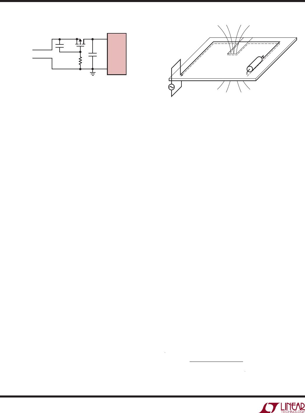
Alternatively, the following soft connect circuit (Figure 6)
can be employed. In this circuit, capacitor C1 holds MP1
off when the cable is first connected. Eventually C1 begins
to charge up to the USB input voltage applying increasing
gate support to MP1. The long time constant of R1 and
C1 prevent the current from building up in the cable too
fast thus dampening out any resonant overshoot.
Printed Circuit Board Layout Considerations
In order to be able to deliver maximum current under all
conditions, it is critical that the Exposed Pad on the back-
side of the LTC3555 family package be soldered to the PC
board ground. Failure to make thermal contact between
the Exposed Pad on the backside of the package and the
copper board will result in higher thermal resistances.
Furthermore, due to its high frequency switching circuitry,
it is imperative that the input capacitors, inductors and
output capacitors be as close to the LTC3555 family as
possible and that there be an
unbroken
ground plane under
the IC and all of its external high frequency components.
APPLICATIONS INFORMATION
LTC3555/LTC3555-X
30
3555fe
For more information www.linear.com/LTC3555
High frequency currents, such as the V
BUS
, V
IN1
, V
IN2
and V
IN3
currents on the LTC3555 family, tend to find
their way along the ground plane in a myriad of paths
ranging from directly back to a mirror path beneath the
incident path on the top of the board. If there are slits or
cuts in the ground plane due to other traces on that layer,
the current will be forced to go around the slits. If high
frequency currents are not allowed to flow back through
their natural least-area path, excessive voltage will build
up and radiated emissions will occur. There should be a
group of vias under the grounded backside of the pack-
age leading directly down to an internal ground plane. To
minimize parasitic inductance, the ground plane should
be on the second layer of the PC board.
The GATE pin for the external ideal diode controller has
extremely limited drive current. Care must be taken to
minimize leakage to adjacent PC board traces. 100nA of
leakage from this pin will introduce an offset to the 15mV
ideal diode of approximately 10mV. To minimize leakage,
the trace can be guarded on the PC board by surrounding
it with V
OUT
connected metal, which should generally be
less that one volt higher than GATE.
When laying out the printed circuit board, the following
checklist should be used to ensure proper operation of
the LTC3555 family.
1. Are the capacitors at V
BUS
, V
IN1
, V
IN2
and V
IN3
as close
as possible to the LTC3555? These capacitors provide
the AC current to the internal power MOSFETs and their
drivers. Minimizing inductance from these capacitors
to the LTC3555 is a top priority.
2. Are C
OUT
and L1 closely connected? The () plate of
C
OUT
returns current to the GND plane.
3. Keep sensitive components away from the SW pins.
Battery Charger Stability Considerations
The LTC3555 familys battery charger contains both a
constant-voltage and a constant-current control loop. The
constant-voltage loop is stable without any compensation
when a battery is connected with low impedance leads.
Excessive lead length, however, may add enough series
inductance to require a bypass capacitor of at least 1µF
from BAT to GND. Furthermore, when the battery is dis-
connected, a 100µF MLCC capacitor in series with a 0.3Ω
resistor from BAT to GND is required to prevent oscillation.
High value, low ESR multilayer ceramic chip capacitors
reduce the constant-voltage loop phase margin, possibly
resulting in instability. Ceramic capacitors up to 22µF
may be used in parallel with a battery, but larger ceramics
should be decoupled with 0.2Ω to of series resistance.
In constant-current mode, the PROG pin is in the feed-
back loop rather than the battery voltage. Because of the
additional pole created by any PROG pin capacitance,
capacitance on this pin must be kept to a minimum. With
no additional capacitance on the PROG pin, the battery
charger is stable with program resistor values as high
as 25k. However, additional capacitance on this node
reduces the maximum allowed program resistor. The pole
frequency at the PROG pin should be kept above 100kHz.
Therefore, if the PROG pin has a parasitic capacitance,
C
PROG
, the following equation should be used to calculate
the maximum resistance value for R
PROG
:
R
PROG
1
2π 100kHz C
PROG
APPLICATIONS INFORMATION
Figure 6. USB Soft Connect Circuit
Figure 7. Higher Frequency Ground Currents Follow Their
Incident Path. Slices in the Ground Plane Cause High Voltage
and Increased Emissions
R1
40k
5V USB
INPUT
3555 F06
C1
100nF
C2
10µF
MP1
Si2333
USB CABLE
V
BUS
GND
LTC3555/
LTC3555-X
3555 F07

LTC3555IUFD#TRPBF

Mfr. #:
Manufacturer:
Analog Devices / Linear Technology
Description:
Battery Management Hi Eff USB Pwr Manager + 3x Buck DC/DC
Lifecycle:
New from this manufacturer.
Delivery:
DHL FedEx Ups TNT EMS
Payment:
T/T Paypal Visa MoneyGram Western Union