MAX7302
SMBus/I
2
C Interfaced 9-Port,
Level-Translating GPIO and LED Driver with CLA
______________________________________________________________________________________ 13
When debouncing is enabled for a port input, transition
detection applies to the stored debounced input signal
value, rather than to the instantaneous value at the
input. This process allows for useful transition detection
of noisy signals, such as keyswitch inputs, without
causing spurious interrupts.
Port Input Transition Detection and Interrupt
Any transition on ports configured as inputs automatically
set the D1 bit of that port’s I/O registers high. Any input can
be selected to assert an interrupt output indicating a transi-
tion has occurred at the input port(s). The MAX7302 sam-
ples the port input (internally latched into a snapshot
register) during a read access to its port P_ I/O register.
The MAX7302 continuously compares the snapshot with
the port’s input condition. If the device detects a change
for any port input, an internal transition flag sets for that
port. Read register 0x26 to clear the interrupt, then read all
the port I/O registers (0x01 to 0x09) by initiating a burst
read to clear the MAX7302’s internal transition flag. Note
that when debouncing is enabled for a port input, transition
detection applies to the stored debounced input signal
value, rather than to the instantaneous value at the input.
Transition bits D4 and D3 must be set to 0 to detect the
next rising or falling edge on the input port P_.
The MAX7302 allows the user to select the input port(s)
that cause an interrupt on the INT output. Set INT for
each port by using the INTenable bit (bit D5) in each
port P_ register. The appropriate port’s transition flag
always sets when an input changes, regardless of the
port’s INTenable bit settings. The INTenable bits allow
processor interrupt only on critical events, while the
inputs and the transition flags can be polled periodical-
ly to detect less critical events.
When debounce is disabled, signal transtions between
the 9th and 11th falling edges of clock will not be regis-
tered since the transition is detected and cleared at the
same read cycle.
Ports configured as outputs do not feature transition
detection, and therefore, cannot cause an interrupt.
The exception to this rule is the CLA outputs.
The INT output never reasserts during a read sequence
because this process could cause a recursive reentry
into the interrupt service routine. Instead, if a data
change occurs during the read that would normally set
the INT output, the interrupt assertion is delayed until
the STOP condition. If the changed input data is read
before the STOP condition, a new interrupt is not
required and not asserted. The INT bit and INT output
(if selected) have the same value at all times.
Transition Flag
The Transition bit in device configuration register 0x26 is
a NOR of all the port I/O registers’ individual Transition
bits. A port I/O register’s Transition bit sets when that
port is set as an input, and the input changes from the
port’s I/O registers last read through the serial interface.
A port’s individual Transition bit clears by reading that
port’s I/O register. The Transition flag of configuration
register 0x26 is only cleared after reading all port I/O
registers on which a transition has occurred.
RST
Input
The active-low RST input operates as a hardware reset
which voids any on-going I
2
C transaction involving the
MAX7302. This feature allows the MAX7302 supply cur-
rent to be minimized in power critical applications by
effectively disconnecting the MAX7302 from the bus.
RST also operates as a chip enable, allowing multiple
devices to use the same I
2
C slave address if only one
MAX7302 has its RST input high at any time. RST can
be configured to restore all port registers to the power-
up settings by setting bit D0 of device configuration reg-
ister 0x26 (Table 1). RST can also be configured to reset
the internal timing counters used for PWM and blink by
setting bit D1 of device configuration register 0x26.
When RST is low, the MAX7302 is forced into the I
2
C
STOP condition. The reset action does not clear the
interrupt output INT. The RST input is referenced to V
DD
and is overvoltage tolerant up to the supply voltage, V
LA
.
REGISTER DATA
ADDRESS
CODE
D7 D6 D5 D4 D3 D2 D1 D0
0x72
Port
P5
Port
P4
Port
P3
Port
P2
Port
P1
Configuration
register 0x27
0
0x73
Port
P9
Port
P8
Port
P7
Port
P6
Table 8. Port Lock Registers
MAX7302
SMBus/I
2
C Interfaced 9-Port,
Level-Translating GPIO and LED Driver with CLA
14 ______________________________________________________________________________________
INT
Output
Port P1 can be configured as a latching interrupt out-
put, INT, that flags any transients on any combination of
selected ports configured as inputs. Configurable logic
gate outputs can also be monitored as readback inputs
with the same options as normal I/O port inputs. Any
transitions occurring at the selected inputs assert INT
low to alert the host processor of data changes at the
selected inputs. Reset INT by reading any ports I/O
registers (0x01 to 0x09).
Standby Mode
Upon power-up, the MAX7302 enters standby mode
when the serial interface is idle. If any of the PWM
intensity control, blink, or debounce features are used,
the operating current rises because the internal PWM
oscillator is running and toggling counters. When using
OSCIN to override the internal oscillator, the operating
current varies according to the frequency at OSCIN.
When the serial interface is active, the operating cur-
rent also increases because the MAX7302, like all I
2
C
slaves, has to monitor every transmission. The bus
timeout and debounce circuits use the internal oscilla-
tor even if OSCIN is selected.
Internal Oscillator and OSCIN/OSCOUT
External Clock Options
The MAX7302 contains an internal 32kHz oscillator. The
MAX7302 always uses the internal oscillator for bus
timeout and for debounce timing (when enabled). It is
used by default to generate PWM and blink timing. The
internal oscillator only runs when the clock output
OSCOUT is needed to keep the operating current as
low as possible.
The MAX7302 can use an external clock source instead
of the internal oscillator for the PWM and blink timing.
The external clock can range from DC to 1MHz, and it
connects to the P2/OSCIN port. The P3/OSCOUT port
provides a buffered and level-shifted output of the inter-
nal oscillator or external clock to drive other devices.
Select the P2/OSCIN and P3/OSCOUT port options
using the device configuration register 0x67 bits D2
and D3 (see Table 4).
The P2/OSCIN port is overvoltage protected to supply
voltage V
LA
, so the external clock can exceed V
DD
if
V
LA
is greater than V
DD
. The port P2 register (see
Tables 2 and 6) sets the P2/OSCIN logic threshold
(30%/70%) to either the V
DD
supply or the V
LA
.
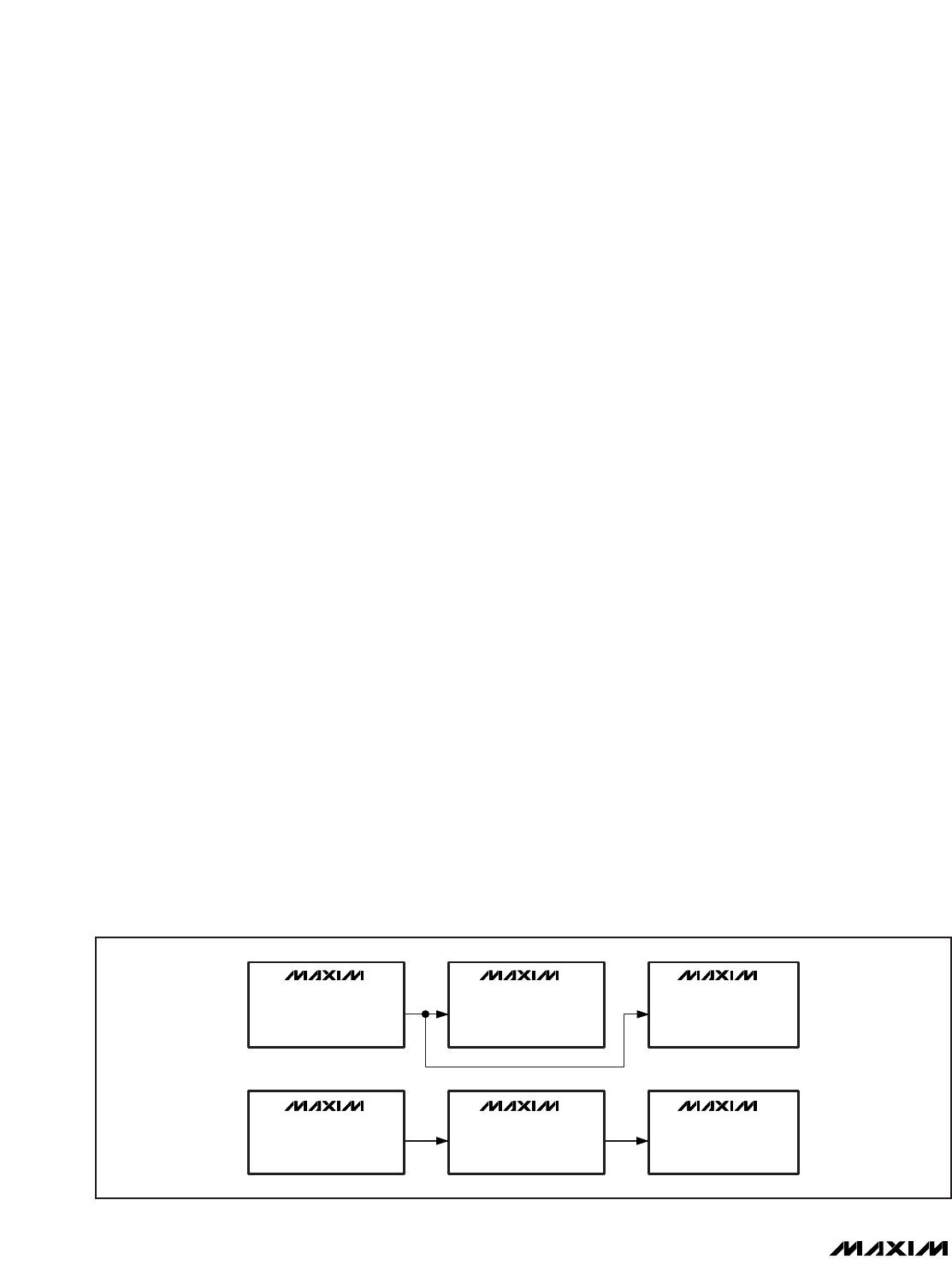
Use OSCOUT or an external clock source to cascade
up to four MAX7302s per master for applications requir-
ing additional ports. To synchronize the blink action
across multiple MAX7302s (see Figures 4 and 5), use
OSCOUT from one MAX7302 to drive OSCIN of the
other MAX7302s. This process ensures the same blink
frequency of all the devices, but also make sure to syn-
chronize the blink phase. The blink timing of multiple
MAX7302s is synchronous at the instant of power-up
because the blink and PWM counters clear by each
MAX7302’s internal reset circuit, and by default the
MAX7302s’ internal oscillators are off upon power-up.
Ensure that the blink phase of all the devices remains
synchronized by programming the OSCIN and
OSCOUT functionality before programming any feature
that causes a MAX7302’s internal oscillator to operate
(blink, PWM, bus timeout, or key debounce). Configure
the RST input to reset the internal timing counters used
for PWM and blink by setting bit D1 of device configu-
ration register 0x26 (see Table 3).
PWM and Blink Timing
The MAX7302 divides the 32kHz nominal internal oscilla-
tor OSC or external clock source OSCIN frequency by 32
to provide a nominal 1kHz PWM frequency. Use the reset
MAX7302
P2/OSCIN
P2/OSCIN
P3/OSCOUT
P2/OSCIN P3/OSCOUT
P2/OSCIN
P3/OSCOUT
MAX7302
MAX7302
MAX7302
MAX7302
MAX7302
Figure 4. Synchronizing Multiple MAX7302s (Internal Oscillator)
MAX7302
SMBus/I
2
C Interfaced 9-Port,
Level-Translating GPIO and LED Driver with CLA
______________________________________________________________________________________ 15
function to synchronize multiple MAX7302s that are oper-
ating from the same OSCIN, or to synchronize a single
MAX7302’s blink timing to an external event. Configure
the RST input to reset the internal timing counters used by
PWM and blink by setting bit D1 of the device configura-
tion register 0x26 (see Table 3).
The MAX7302 uses the internal oscillator by default.
Configure port P2 using device configuration register
0x27 bit D2 (see Table 4) as an external clock source
input, OSCIN, if the application requires a particular or
more accurate timing for the PWM or blink functions.
OSCIN only applies to PWM and blink; the MAX7302
always uses the internal oscillator for debouncing and
bus timeout. OSCIN can range up to 1MHz. Use device
configuration register 0x27 bit D3 (see Table 4) to con-
figure port P3 as OSCOUT to output a MAX7302’s
clock. The MAX7302 buffers the clock output of either
the internal oscillator OSC or the external clock source
OSCIN, according to port D2’s setup. Synchronize mul-
tiple MAX7302s without using an external clock source
input by configuring one MAX7302 to generate
OSCOUT from its internal clock, and use this signal to
drive the remaining MAX7302s’ OSCIN.
A PWM period contains 32 cycles of the nominal 1kHz
PWM clock (see Figure 6). Set ports individually to a
PWM duty cycle between 0/32 and 31/32. For static
logic-level low output, set the ports to 0/32 PWM, and
for static logic-level high output, set the port register to
0111XXXX (see Table 9). The MAX7302 staggers the
PWM timing of the 9-port outputs, in single or dual
ports, by 1/8 of the PWM period. These phase shifts
distribute the port-output switching points across the
PWM period (see Figure 7). This staggering reduces
the di/dt output-switching transient on the supply and
also reduces the peak/mean current requirement.
All ports feature LED blink control. A global blink period
of 1/8s, 1/4s, 1/2s, 1s, 2s, 4s, or 8s applies to all ports
(see Table 10). Any port can blink during this period
with a 1/16 to 15/16 duty cycle, adjustable in 1/16
increments (see Table 11). For PWM fan control, the
MAX7302 can set the blink frequency to 32Hz.
P2/OSCIN
EXTERNAL
OSCILLATOR
EXTERNAL
OSCILLATOR
0 TO 1MHz
P2/OSCIN P2/OSCIN
P2/OSCIN
P3/OSCOUT
0 TO 1MHz
P2/OSCIN P3/OSCOUT P2/OSCIN
MAX7302
MAX7302
MAX7302
MAX7302
MAX7302
MAX7302
Figure 5. Synchronizing Multiple MAX7302s (External Clock)
REGISTER DATA
PWM SETTINGS
D7 D6 D5 D4 D3 D2 D1 D0
Port P_ is a static logic-level low output port 0 X 0 0 0 0 0 0
Port P_ is a PWM output port; PWM duty cycle is 1/32 0 X 0 0 0 0 0 1
Port P_ is a PWM output port; PWM duty cycle is 2/32 0 X 0 0 0 0 1 0
Port P_ is a PWM output port; PWM duty cycle is 3/32 0 X 0 0 0 0 1 1
Port P_ is a PWM output port; PWM duty cycle is 4/32 0 X 0 0 0 1 0 0
……
Port P_ is a PWM output port; PWM duty cycle is 30/32 0 X 0 1 1 1 1 0
Port P_ is a PWM output port; PWM duty cycle is 31/32 0 X 0 1 1 1 1 1
Port P_ is a static logic-level high output port 0 1 1 1 X X X X
Table 9. PWM Settings on Output Port

MAX7302ATE+T

Mfr. #:
Manufacturer:
Maxim Integrated
Description:
Interface - I/O Expanders 9-Port Level-Trans GPIO & LED Driver
Lifecycle:
New from this manufacturer.
Delivery:
DHL FedEx Ups TNT EMS
Payment:
T/T Paypal Visa MoneyGram Western Union