MAX7302
SMBus/I
2
C Interfaced 9-Port,
Level-Translating GPIO and LED Driver with CLA
16 ______________________________________________________________________________________
HIGH-Z
LOW
HIGH-Z
LOW
HIGH-Z
LOW
OUTPUT LOW 31/32 DUTY PWM
HIGH-Z
LOW
HIGH-Z
LOW
HIGH-Z
LOW
OUTPUT LOW 30/32 DUTY PWM
OUTPUT STATIC LOW (STATIC LOGIC-LOW OUTPUT OR LED DRIVE ON)
OUTPUT LOW 2/32 DUTY PWM
0b0X000000
OUTPUT STATIC HIGH (STATIC LOGIC-HIGH OUTPUT OR LED DRIVE OFF)
HIGH-Z
LOW
OUTPUT LOW 3/32 DUTY PWM
HIGH-Z
LOW
OUTPUT LOW 29/32 DUTY PWM
PORT
REGISTER
VALUE
977μs NOMINAL PWM PERIOD (1024Hz PERIOD)
0b0X000010
0b0X000011
0b0X011101
0b0X011110
0b0X011111
0b0111XXXX
0b0X000001
OUTPUT LOW 1/32 DUTY PWM
Figure 6. Static and PWM Port Output Waveforms
012
977μs NOMINAL PWM PERIOD
OUTPUT P8
345678
OUTPUT P8 OUTPUT P8
OUTPUTS P1, P9 OUTPUTS P1, P9 OUTPUTS P1, P9
OUTPUT P2 OUTPUT P2 OUTPUT P2
OUTPUT P3 OUTPUTP3 OUTPUT P3
OUTPUT P4 OUTPUT P4
OUTPUT P5 OUTPUT P5
OUTPUT P6 OUTPUT P6
OUTPUT P7 OUTPUT P7
NEXT PWM PERIOD NEXT PWM PERIOD
Figure 7. Staggered PWM Phasing Between Port Outputs
MAX7302
SMBus/I
2
C Interfaced 9-Port,
Level-Translating GPIO and LED Driver with CLA
______________________________________________________________________________________ 17
REGISTER DATA
PWM SETTINGS
D7 D6 D5 D4 D3 D2 D1 D0
Port P_ is a static logic-level low output port 0 X 1 00000
Port P_ is a PWM output port; PWM duty cycle is 1/16 0 X 1 00001
Port P_ is a PWM output port; PWM duty cycle is 2/16 0 X 1 00010
Port P_ is a PWM output port; PWM duty cycle is 3/16 0 X 1 00100
……
Port P_ is a PWM output port; PWM duty cycle is 14/16 0 X 1 0 1 1 1 0
Port P_ is a PWM output port; PWM duty cycle is 15/16 0 X 1 0 1 1 1 1
Port P_ is a static logic-level high output port (32/32) 0 1 1 1 X X X X
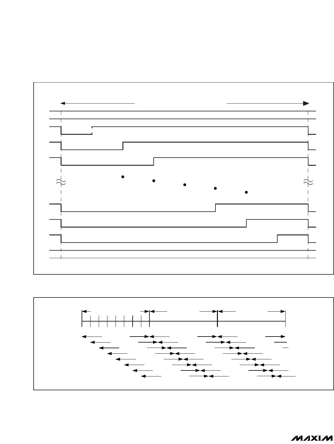
Table 11. Blink Settings on Output Ports
REGISTER BIT
FUNCTION
D5 D4 D3 D2 D1 D0
XOR noninverted 00
XOR P3 inverted 10
XOR P2 inverted 01
XOR both ports inverted
01X
1
X
1
3 input AND/OR all noninverted 0 0 0
3 input AND/OR P2 inverted 0 0 1
3 input AND/OR P3 inverted 0 1 0
3 input AND/OR P4 inverted 0 1 1
3 input AND/OR P2 and P3 inverted 1 0 0
3 input AND/OR P2 and P4 inverted 1 0 1
3 input AND/OR P3 and P4 inverted 1 1 0
3 input AND/OR all inverted
1
1
1
1
1
1
Table 12. CLA0 (P2–P5) Configuration Register Setting (0x28)
DEVICE CONFIGURATION
REGISTER 0x26
BLINK OR PWM SETTING
BIT D4
BLINK2
BIT D3
BLINK1
BIT D2
BLINK0
BLINK OR PWM
FREQUENCY (32kHz
INTERNAL OSCILLATOR)
(Hz)
BLINK OR PWM
FREQUENCY (0 TO 1MHz
EXTERNAL OSCILLATOR)
Bl i nk p er i od i s 8s ( 0.125H z) 0 0 0 0.125 OSCIN / 262,144
Blink period is 4s (0.25Hz) 0 0 1 0.25 OSCIN / 131,072
Blink period is 2s (0.5Hz) 0 1 0 0.5 OSCIN / 65,536
Blink period is 1s (1Hz) 0 1 1 1 OSCIN / 32,768
Blink period is a 1/2s (2Hz) 1 0 0 2 OSCIN / 16,384
Blink period is a 1/4s (4Hz) 1 0 1 4 OSCIN / 8192
Bl i nk p er i od i s an 1/8s ( 8H z) 1 1 0 8 OSCIN / 4096
Bl i nk p er i od i s a 1/32s ( 32H z) 1 1 1 32 OSCIN / 1024
PWM X X X 1024 OSCIN / 32
Table 10. Blink and PWM Frequencies
MAX7302
SMBus/I
2
C Interfaced 9-Port,
Level-Translating GPIO and LED Driver with CLA
18 ______________________________________________________________________________________
BIT
LOGIC LEVEL
FUNCTION
0 Output not cascaded to CLA1
D7
1 Output cascaded to CLA1
0 Output noninverted
D6
1 Output inverted
Table 13. Output P5 Configuration
REGISTER BIT
FUNCTION
D5 D4 D3 D2 D1 D0
2 input AND/OR P2 and P3 noninverted 0 0
2 input AND/OR P2 and P3 inverted 1 0
2 input AND/OR P2 inverted and P3 0 1
2 input AND/OR P2 and P3 both inverted
0X1
1
1
1
2 input AND/OR P2 and P4 noninverted 0 0
2 input AND/OR P2 and P4 inverted 1 0
2 input AND/OR P2 inverted and P4 0 1
2 input AND/OR P2 and P4 both inverted
1
1
0X1
1
2 input AND/OR P3 and P4 noninverted 0 0
2 input AND/OR P3 and P4 inverted 0 1
2 input AND/OR P3 inverted and P4 1 0
2 input AND/OR P3 and P4 both inverted
1
1
1
1
0X
Table 12. CLA0 (P2–P5) Configuration Register Setting (0x28) (continued)
REGISTER BIT
FUNCTION
D5 D4 D3 D2 D1 D0
XOR noninverted 00
XOR P7 inverted 10
XOR P6 inverted 01
XOR both ports inverted
01X
1
X
1
3 input AND/OR all noninverted 0 0 0
3 input AND/OR P6 inverted 0 0 1
3 input AND/OR P7 inverted 0 1 0
3 input AND/OR P8 inverted 0 1 1
3 input AND/OR P6 and P7 inverted 1 0 0
3 input AND/OR P6 and P8 inverted 1 0 1
3 input AND/OR P7 and P8 inverted 1 1 0
3 input AND/OR all inverted
1
1
1
1
1
1
2 input AND/OR P6 and P7 noninverted 0 0
2 input AND/OR P6 and P7 inverted 1 0
2 input AND/OR P6 inverted and P7 0 1
2 input AND/OR P6 and P7 both inverted
0X1
1
1
1
Table 14. CLA1 (P6–P9) Configuration Register Setting (0x29)

MAX7302ATE+T

Mfr. #:
Manufacturer:
Maxim Integrated
Description:
Interface - I/O Expanders 9-Port Level-Trans GPIO & LED Driver
Lifecycle:
New from this manufacturer.
Delivery:
DHL FedEx Ups TNT EMS
Payment:
T/T Paypal Visa MoneyGram Western Union