MAX7302
SMBus/I
2
C Interfaced 9-Port,
Level-Translating GPIO and LED Driver with CLA
______________________________________________________________________________________ 19
REGISTER DATA
REGISTER
D7–D2
D1 D0
CLA0 and CLA1 configurable
logic enable
CLA1
CLA0
Ports P2–P5 are GPIO ports X 0
Ports P2–P5 are configurable logic
CLA0
—X 1
Ports P6–P9 are GPIO ports 0 X
Ports P6–P9 are configurable logic
CLA1
—1 X
Table 16. Configurable Logic-Array
Enable Register (0x70)
BIT
LOGIC LEVEL
FUNCTION
0 Cascade input noninverted
D7
1 Cascade input inverted
0 Output noninverted
D6
1 Output inverted
Table 15. Output P9 and Cascade P5
Input Configuration
REGISTER BIT
FUNCTION
D5 D4 D3 D2 D1 D0
2 input AND/OR P6 and P8 noninverted 0 0
2 input AND/OR P6 and P8 inverted 1 0
2 input AND/OR P6 inverted and P8 0 1
2 input AND/OR P6 and P8 both inverted
1
1
0X1
1
2 input AND/OR P7 and P8 noninverted 0 0
2 input AND/OR P7 and P8 inverted 0 1
2 input AND/OR P7 inverted and P8 1 0
2 input AND/OR P7 and P8 both inverted
1
1
1
1
0X
Table 14. CLA1 (P6–P9) Configuration Register Setting (0x29) (continued)
REGISTER DATA
REGISTER
D7–D2
D1 D0
CLA0 and CLA1 configurable
logic lock
CLA1
CLA0
CLA0 is not locked X 0
CLA0 is locked X 1
CLA1 is not locked 0 X
CLA1 is locked 1 X
Table 17. Configurable Logic-Array Lock
Register (0x71)
MAX7302
SMBus/I
2
C Interfaced 9-Port,
Level-Translating GPIO and LED Driver with CLA
20 ______________________________________________________________________________________
REGISTER BIT DESCRIPTION
VALUE
FUNCTION
D7 Don’t care x Don’t care.
0 Refers inputs to the VL supply voltage; sets outputs to open drain.
D6
Port supply
reference
1 Refers inputs to the V
DD
supply voltage; sets outputs to push-pull.
0 Disables the transition interrupt.
D5
Transition interrupt
enable
1 Enables the transition interrupt.
D4
Transition detection
bit 1
0 Detects the next transition on the port input.
D3
Transition detection
bit 0
0 Detects the next transition on the port input.
0 Disables debouncing of the input port.
D2 Debounce
1 Enables debouncing of the input port.
0 No transition has occurred since the last port read.
D1
Port transition state
1 A transition has occurred since the last port read.
0 Port input is logic-low.
D0 Port status
1 Port input is logic-high.
Table 18. Port I/O Registers (I/O Port 5 and 9 Configured as CLA Outputs, Registers
0x05 and 0x09)
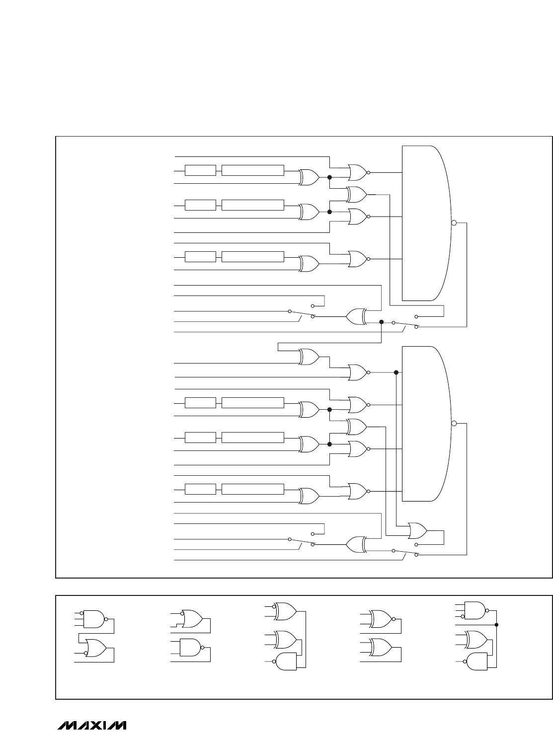
Configurable Logic Array (CLA)
The CLA configures groups of four ports as either a
combinational logic gate up to three inputs, or a two
input exclusive OR/NOR gate (see Tables 12-15).
Eight-port dual groups can be cascaded to form a
two-level gate with the intermediate term brought out
as an output or not, as desired. If fewer than three
gate inputs are needed, the unused CLA input(s)
(which can be any combination of the three CLA
inputs) remain available as independent GPIO ports
(see Figure 8). Use the configurable logic-array enable
register (see Table 16) to enable ports as CLAs. Use the
configurable logic-array lock register (see Table 17) to
permanently lock in any logic-array combination of CLAs
until the next power cycle. Setting D0 and D1 to logic-
high in the configurable logic-array lock register locks the
corresponding bit position in the configurable logic-array
enable register. Additionally, the appropriate CLA_ regis-
ter (addresses 0x28 and 0x29) cannot be changed.
The configurable logic-array lock register is unlocked
on power-up, or by RST when configured by the
RSTPOR bit in the configure register. Each lock bit can
only be written to once per power cycle.
A CLA’s input(s) and output can be read through the
serial interface like a normal input port. The MAX7302
creates a gate that provides an independent real-time
logic function, and every node of it can be examined
through the I
2
C interface with optional debounce and
transition detection.
Setting bits D0 and D1 to logic-high enables the CLA
functionality and sets ports P5 and P9 as CLA outputs
(see Table 16). When in CLA mode, the port I/O regis-
ter data is interpreted differently for CLA output ports
(see Table 18). Bit D7 that normally selects the port
direction is ignored because either port P5 or P9 is
always an output. Bit D6 sets both the CLA output type
(push-pull or open drain) and the logic threshold for
reading the CLA output status back through the I
2
C
interface. The other bits set the readback options, such
as debounce and transition detection interrupt.
MAX7302
SMBus/I
2
C Interfaced 9-Port,
Level-Translating GPIO and LED Driver with CLA
______________________________________________________________________________________ 21
ENABLE P3
INVERT P9
ENABLE P4
INVERT P8
ENABLE P2
INVERT P2
ENABLE P8
INVERT P4
ENABLE P7
INVERT P5
ENABLE P6
INVERT P6
P5 IS CLA/GPIO
INVERT P3
ENABLE P5 CASCADE
INVERT P5 CASCADE
P5 OUTPUT REGISTER
PIN P7
PIN P2
PIN P3
PIN P4
PIN P5
PIN P6
PIN P8
P9 IS CLA/GPIO
INVERT P7
P9 OUTPUT REGISTER
PIN P9
ENABLE EXOR23
ENABLE EXOR67
ENABLE EXOR23 = /D5 * D4 IN CLA REGISTER 0x28
ENABLE EXOR67 = /D5 * D4 IN CLA REGISTER 0x29
P2–P5
[CLA0]
P6–P9
[CLA1]
DEBOUNCE TRANSITION DETECTION
Figure 8. Configurable Logic-Array Structure
P2
P3
P4
P7
P9
EXAMPLE 1:
REGISTER 0x28: DATA VALUE 8’b1011_1110
REGISTER 0x29: DATA VALUE 8’b0000_1100
EXAMPLE 2:
REGISTER 0x28: DATA VALUE 8’b0010_0011
REGISTER 0x29: DATA VALUE 8’b0011_1101
EXAMPLE 3:
REGISTER 0x28: DATA VALUE 8’b1001_1011
REGISTER 0x29: DATA VALUE 8’b1101_1010
EXAMPLE 4:
REGISTER 0x28: DATA VALUE 8’b0101_1010
REGISTER 0x29: DATA VALUE 8’b0001_1010
EXAMPLE 5:
REGISTER 0x28: DATA VALUE 8’b1110_1111
REGISTER 0x29: DATA VALUE 8’b0101_1010
P2
P3
P4
P5
P4
P2
P5
P3
P2
P6
P7
P9
P8
P7
P9
P6
P7
P9
P3
P5
P2
P6
P7
P9
Figure 9. Configurable Logic Examples

MAX7302ATE+T

Mfr. #:
Manufacturer:
Maxim Integrated
Description:
Interface - I/O Expanders 9-Port Level-Trans GPIO & LED Driver
Lifecycle:
New from this manufacturer.
Delivery:
DHL FedEx Ups TNT EMS
Payment:
T/T Paypal Visa MoneyGram Western Union