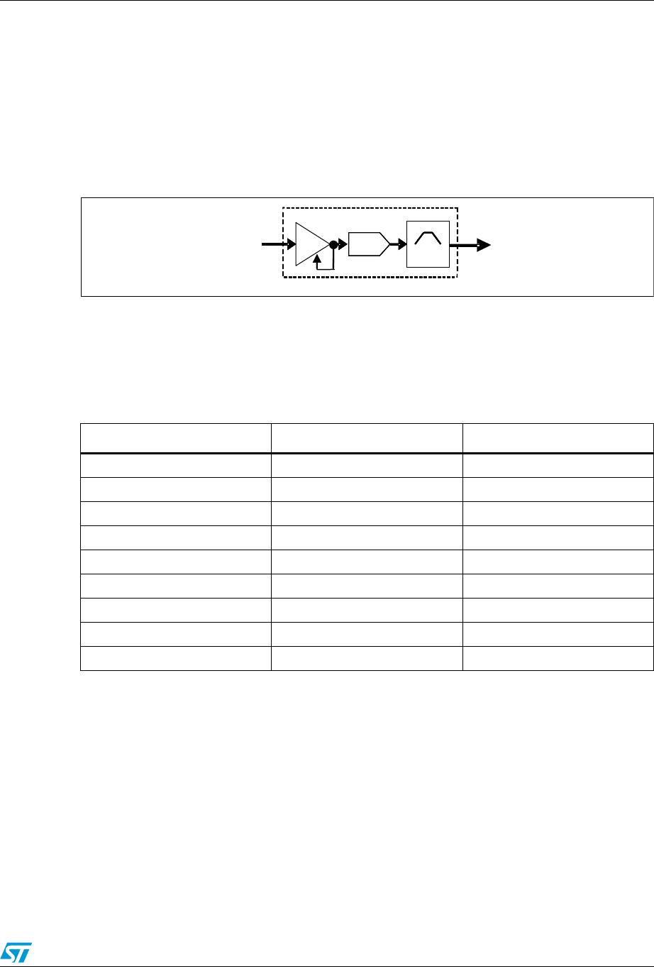
ST7570 Analog front end (AFE)
Doc ID 17526 Rev 2 15/26
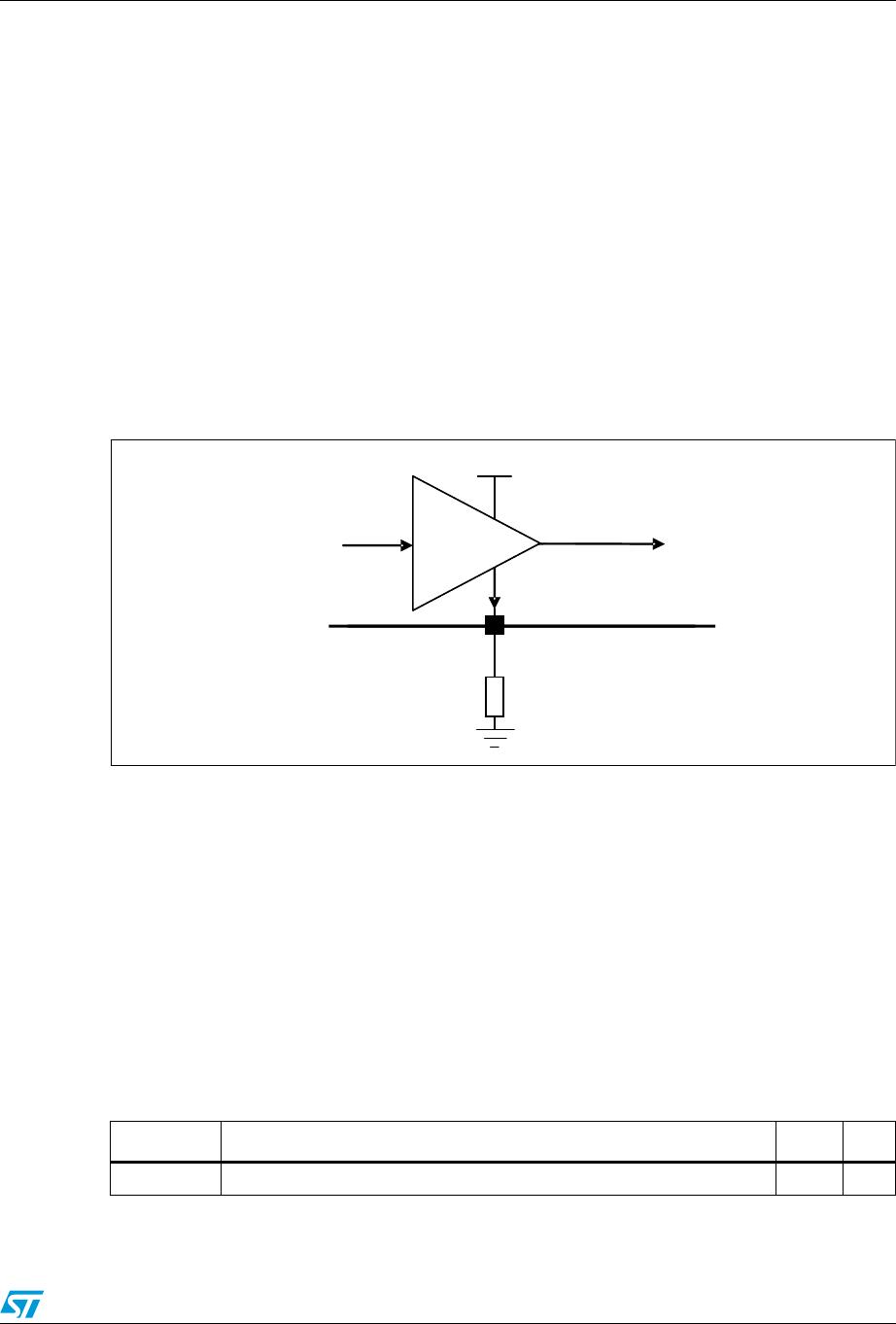
5.4 Current and voltage control
The power amplifier output current sensing is performed by mirroring a fraction of the output
current and making it flow through a resistor R
CL
connected between the C
L
pin and VSS.
The following relationship can be established between V(CL) and I(PA_OUT):
Equation 2 V(CL) vs. I(PA_OUT)
The voltage level V(CL) is compared with the internal threshold CL_TH. When the V(CL)
exceeds the CL_TH level, the V(TX_OUT) voltage is decreased by one TX_GAIN step at a
time until V(CL) goes below the CL_TH threshold.
The current sense circuit is depicted in Figure 6.
Figure 7. PA_OUT current sense circuit
The R
CL
value to get the desired output current limit I(PA_OUT)LIM can be calculated
according to Equation 3:
Equation 3 R
CL
calculation
Note that I(PA_OUT)
LIM
is expressed as peak current, so the corresponding rms current
value shall be calculated according to the transmitted signal waveform.
The R
CL
value to get 1 A rms output current limit, calculated with typical values for CL_TH
and CL_RATIO parameters, is indicated in Ta ble 7.
Table 7. CL resistor typical values
Parameter Description Value Unit
R
CL
Resistor value for I(PA_OUT) MAX = 1 A rms (1.41 A peak) 133 Ω
VCL()
R
CL
I PA_OUT()⋅
CL_RATIO
-------------------------------------------------=
!-V
3$
&/
9&&
&/
,&/ ,3$B287&/B5$7,2
3$
,3$B287
5
R
CL
CL_TH
I(PA_OUT)
LIM
CL_RATIO⁄
---------------------------------------------------------------------------=