Analog front end (AFE) ST7570
16/26 Doc ID 17526 Rev 2
5.5 Thermal shutdown and temperature control
The ST7570 performs an automatic shutdown of the power amplifier circuitry when the
internal temperature exceeds T_TH
4
. After a thermal shutdown event, the temperature must
get below T_TH
3
before the ST7570 power amplifier comes back to operation.
Moreover, a digital thermometer is embedded to identify the internal temperature among
four zones, as indicated in Tabl e 8 .
Table 8. Temperature zones
5.6 Zero-crossing PLL and delay compensation
In operating mode, ST7570 needs to be synchronized with an external signal period through
zero crossing detection.
The user can select among two input pins for the external zero-crossing reference:
Analog input (ZC_IN_A): it requires a bipolar analog input signal which is internally
squared through a Schmidt Trigger comparator with symmetrical thresholds;
Digital input (ZC_IN_D): it requires a 50% duty-cycle square-wave digital signal (with
two levels).
The desired input can be selected by accessing a dedicated management information base
(MIB) object.
The ST7570 embeds a phase-locked loop (PLL) to generate the internal reference based on
the external zero-crossing. In case of delay due to external zero crossing coupling circuits
(i.e. based on optocouplers) or to improve interoperability, it is possible to introduce delay
compensation through a dedicated MIB object.
Figure 8. Zero crossing detection
Temperature zone Temperature value
1T < T_TH
1
2T_TH
1
< T < T_TH
2
3T_TH
2
< T < T_TH
3
4T > T_TH
3
!-V
=&B,1B'
=&B,1B'
FRQILJXUDWLRQ
ELW
0,%REMHFW
,QWHUQDO
5HIHUHQFH
3//
6FKPLGW
7ULJJHU
=&B,1B$
ST7570 Power management
Doc ID 17526 Rev 2 17/26
6 Power management
Figure 9 shows the power supply structure for the ST7570 device. The ST7570 operates
from two external supply voltages:
VCC (8 to 18 V) for the power amplifier and the analog section;
VDDIO (3.3 or 5 V) for interface lines and digital blocks.
Two internal linear regulators provide the remaining required voltages:
5 V analog front end supply: generated from the VCC voltage and connected to the
VCCA pin;
1.8 V digital core supply: generated from the VDDIO voltage and connected to
VDD_REG_1V8 (direct regulator output) and VDD pins.
The VDD_PLL pin, supplying the internal clock PLL, must be externally connected to VDD.
All supply voltages must be properly filtered to their respective ground, using external
capacitors close to each supply pin, in accordance to the supply scheme depicted in
Figure 9.
Note that the internal regulators connected to VDD_REG_1V8 and to VCCA are not
designed to supply external circuitry; their outputs are externally accessible for filtering
purpose only.
Figure 9. Power supply internal scheme
!-V
6##!
633
6$$)/
'.$
6$$?2%'?6
!&%
$)')4!,#/2%
0!
$)')4!,).4%2&!#%3
6$$
633!
6$$?0,,
).4%2.!,0,,
,$/
,$/
6##
63
3!
'.$
Clock management ST7570
18/26 Doc ID 17526 Rev 2
7 Clock management
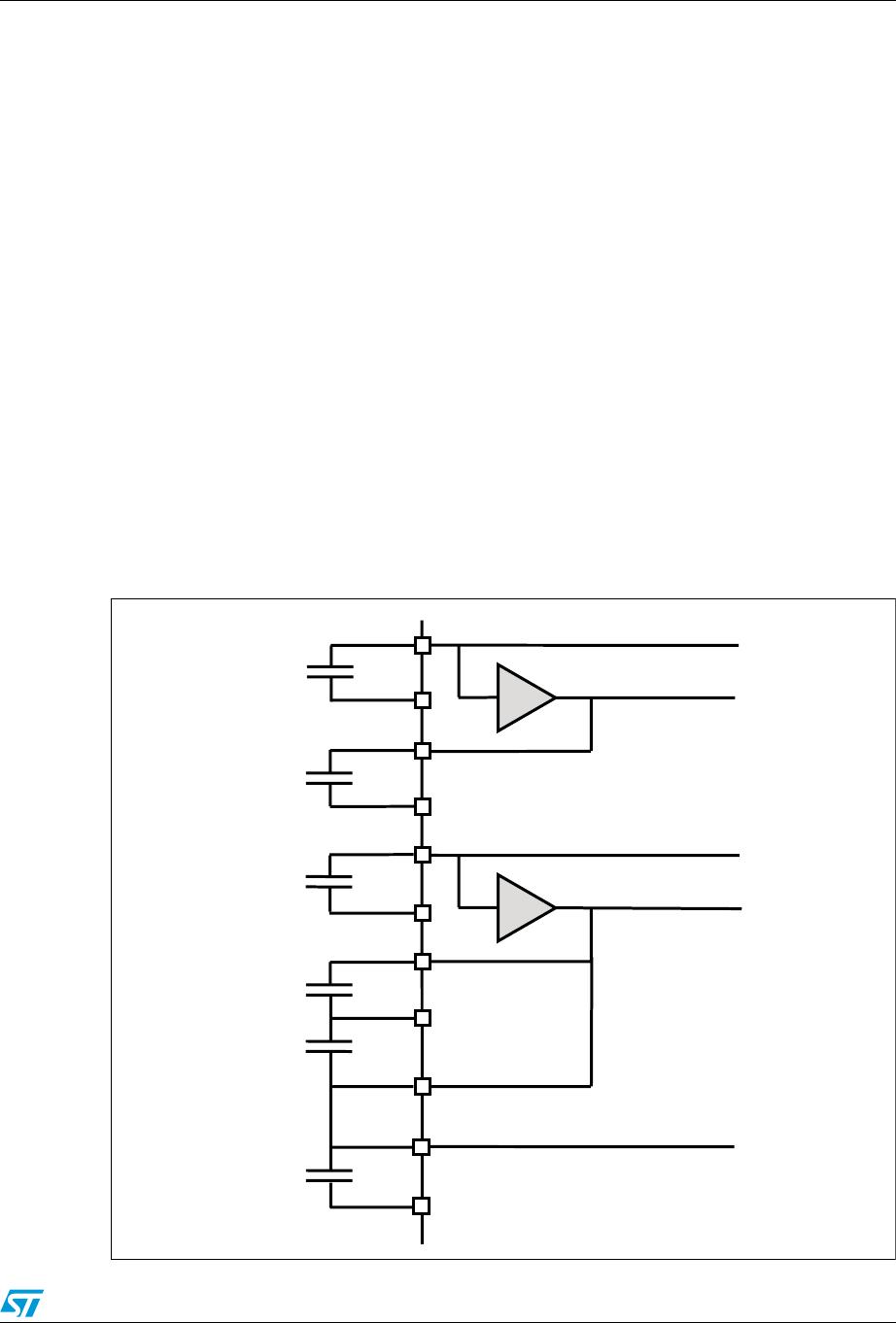
The main clock source is an 8 MHz crystal connected to the internal oscillator through XIN
and XOUT pins. Both XIN and XOUT pins have a 32 pF integrated capacitor, in order to
drive a crystal having a load capacitance of 16 pF with no additional components.
Alternatively, an 8 MHz external clock can be directly supplied to XIN pin, leaving XOUT
floating.
A PLL internally connected to the output of the oscillator generates the f
CLK_PHY
, required by
the PHY processor block. f
CLK_PHY
is then scaled down by two to obtain f
CLK_PC
, required
by the protocol controller.
8 Functional overview
The ST7570 embeds complete physical (PHY) and a medium access control (MAC)
protocol layers and services compliant with the open standard IEC61334-5-1, mainly
developed for smart metering applications, but suitable also for other command and control
applications and remote load management in CENELEC B and D bands.
A local port (UART) is available for communication with an external host, exporting all the
functions and services required to configure and control the device and its protocol stack.
Below a list of the protocol layers and functions embedded in the ST7570 (Figure 10):
Physical layer: implemented in the PHY processor and exporting all the primitive
functions listed in the international standard document IEC61334-5-1, plus additional
services for configuration, alarm management, signal and noise amplitude estimation,
phase detection, statistical information;
MAC layer: implemented on the protocol controller and exporting all the primitive
functions listed in the international standard document IEC61334-5-1, Repeater Call
and Intelligent search initiator process together with additional services.
Management information base (MIB): an information database with all the data
required for proper configuration of the system (at both PHY and MAC layer);
Host interface: all the services of the PHY, MAC and MIB are exported to an external
host through the local UART port.

ST7570TR

Mfr. #:
Manufacturer:
STMicroelectronics
Description:
Network Controller & Processor ICs S-FSK Power Line SOC PHY 2.4 kpbs
Lifecycle:
New from this manufacturer.
Delivery:
DHL FedEx Ups TNT EMS
Payment:
T/T Paypal Visa MoneyGram Western Union

Products related to this Datasheet