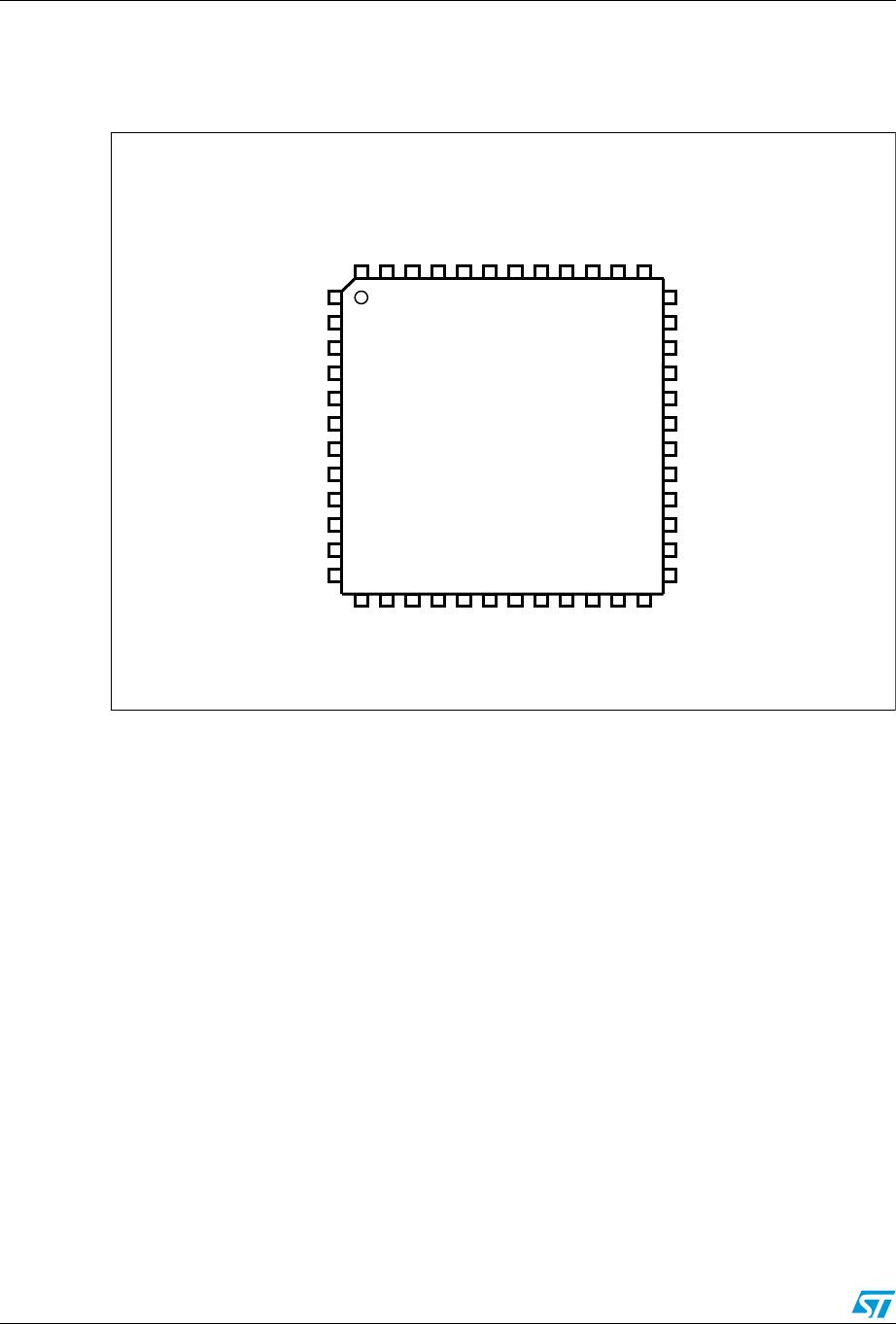
Pin connection ST7570
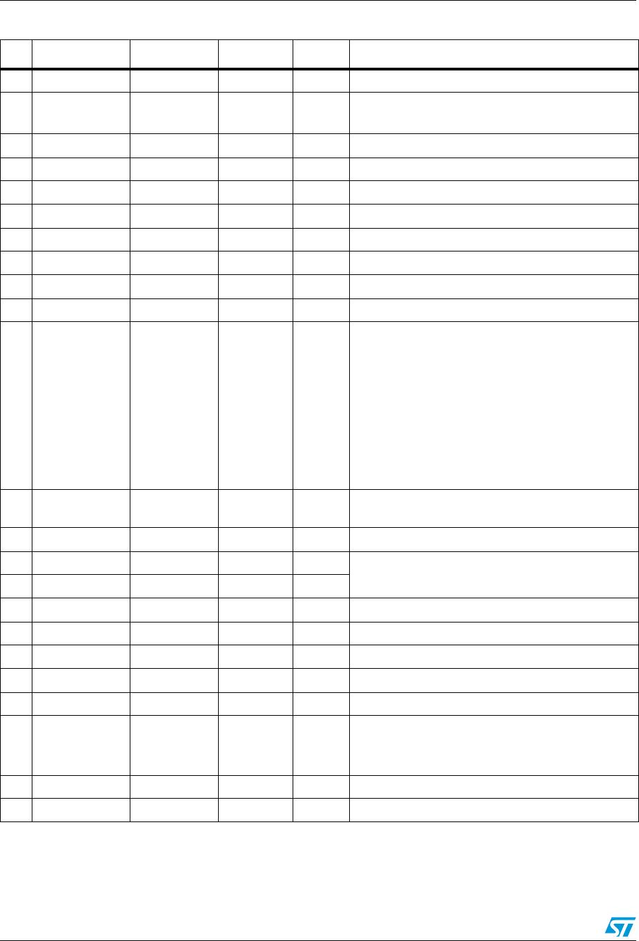
6/26 Doc ID 17526 Rev 2
26 PA_OUT Analog output - - Power amplifier output
27 VDD_REG_1V8 Power - -
1.8 V digital supply / internal regulator output
Externally accessible for filtering purposes only
28 VDDIO Power - - 3.3 V – 5 V I/O external supply
29 NC - - - Not used, leave floating
30 NC - - - Not used, leave floating
31 RESERVED6 - - - Pull up to VDDIO
32 NC - - - Not used, leave floating
33 GND Power - - Digital ground
34 VDDIO Power - - 3.3 V – 5 V I/O supply
35 VSSA Power - - Analog ground
36
PRESLOT
/ZC/TS/BIT
Digital output High Z Disabled
Configurable digital output:
- Slot synchronization (PRESLOT),
- Zero Crossing (ZC),
- Timeslot (TS),
- Bit synchronization (BIT),
- Transmission in progress (TXP),
- Reception in progress (RXP),
- Transmission or Reception in progress (TXRXP).
If not used, this pin can be left floating.
37 ZC_IN_D Digital input High Z Disabled
Digital zero-crossing input.
Pull up to VDDIO if not used
38 T_REQ Digital input High Z Disabled UART communication control line
39 BR1 Digital input High Z Disabled
UART baud rate selection
(sampled after each reset event) see Tab l e 3
40 BR0 Digital input High Z Disabled
41 RESERVED0 - - - Connect to GND
42 RESERVED1 - - - Pull up to VDDIO
43 RESERVED2 - - - Pull up to VDDIO
44 RESERVED3 - - - Pull up to VDDIO
45 GND Power - - Digital ground
46 VDD Power - -
1.8 V digital supply.
Internally connected to VDD_REG_1V8
Externally accessible for filtering purposes only
47 RESERVED4 - - - Connect to VDDIO
48 RESERVED5 - - - Pull up to VDDIO
Table 2. Pin description (continued)
Pin Name Type Reset state Pull-up Description