General Description
The MAX5058/MAX5059 enable secondary-side syn-
chronous rectification in isolated power supplies using
widely available power MOSFETs. These devices facili-
tate the commutation of the secondary-side MOSFETs by
providing a clean gate-drive signal that is synchronized
to the power MOSFET switching in the primary side of
the isolation transformer. The MAX5058/MAX5059 com-
plement the MAX5051 and MAX5042/MAX5043 primary-
side PWM ICs and enable the design of high-efficiency
synchronously rectified isolated power supplies.
Simultaneous conduction of the primary side and the
freewheeling synchronous rectifier MOSFET is avoided
by having a look-ahead signal (before the primary-side
MOSFETs turn ON), thus eliminating large current spikes
resulting from a shorted transformer secondary.
An on-board error amplifier with a versatile current ref-
erence output enables virtually unlimited possibilities in
reference-voltage generation. Reference voltage for the
error amplifier is generated by connecting an appropri-
ate resistor to this output.
Low on-resistance margining MOSFETs integrated on-
chip allow for implementation of a margining circuit
without the use of external switches. The MAX5058 pro-
vides a 5V LDO output for logic-level MOSFETs while
the MAX5059 provides a 10V LDO output for conven-
tional 10V MOSFETs.
The MAX5058/MAX5059 are designed to enable paral-
leling of multiple power supplies for accurate current
sharing using a simple 2-wire, differential, current-share
bus. Parallelability enables expansion of the power
capabilities and simplifies thermal management in high-
output-current applications. When used in conjunction
with the MAX5051, the primaries can also be synchro-
nized and operated 180 degrees out of phase.
The MAX5058/MAX5059 are available in a 28-pin ther-
mally enhanced TSSOP package and operate over a
wide -40°C to +125°C temperature range.
Warning: The MAX5058/MAX5059 are designed to
work in circuits that contain high voltages. Exercise
caution.
Applications
Isolated Telecom Power Supplies
Isolated Networking Power Supplies
±48V Power-Supply Modules
Industrial Power Supplies
±48V/±12V Server Power Supplies
Features
Clean Drive Waveforms for Synchronous
MOSFETs
Utilization of a Look-Ahead Signal from the
Primary for Proper Turn-On/Turn-Off Times
Synchronous Rectifier Drivers Capable of
Sourcing and Sinking Up to 2A Peak Current
Internal Gate-Voltage Regulator for 5V (MAX5058)
or 10V (MAX5059) Gate-Drive Voltage
Internal Error Amplifier
Accurate Differential Current-Share/Force Circuit
Allows Paralleling of Several Power Supplies for
High Output Current
Internal Remote Voltage-Sense Amplifier
Flexible Reference-Voltage Generation
Output Voltage Regulation Down to 0.5V
Low Quiescent Current Consumption of 2.5mA
Integrated Digital Output Margining Circuit Saves
External Parts and Board Space
30ns Propagation Delay Time from Pulse Input
to Output
Automatic Detection of Discontinuous Current
Conduction and Turn-Off of the Freewheeling
MOSFET
High Efficiency at Low Output Currents and
Reverse-Current Protection
Open-Drain Overtemperature Warning Flag
28-Pin Thermally Enhanced TSSOP Package
MAX5058/MAX5059
Parallelable Secondary-Side Synchronous Rectifier
Driver and Feedback-Generator Controller ICs
________________________________________________________________ Maxim Integrated Products 1
19-3045; Rev 0; 10/03
For pricing, delivery, and ordering information, please contact Maxim/Dallas Direct! at
1-888-629-4642, or visit Maxim’s website at www.maxim-ic.com.
Pin Configuration appears at end of data sheet.
EVALUATION KIT
AVAILABLE
Ordering Information
PART
TEMP RANGE
PIN-
PACKAGE
V
REG
(V)
MAX5058AUI -40°C to +125°C 28 TSSOP-EP*
5
MAX5058EUI
-40°C to +85°C 28 TSSOP-EP*
5
MAX5059AUI -40°C to +125°C 28 TSSOP-EP*
10
MAX5059EUI
-40°C to +85°C 28 TSSOP-EP*
10
*EP = Exposed paddle.
MAX5058/MAX5059
Parallelable Secondary-Side Synchronous Rectifier
Driver and Feedback-Generator Controller ICs
2 _______________________________________________________________________________________
ABSOLUTE MAXIMUM RATINGS
ELECTRICAL CHARACTERISTICS
(V+ = +12V, GND = PGND = 0, VDR = V
REG
, C
QSYNC
= C
QREC
= 0, ZCP = ZCN = BUFIN = CSP = CSN = SFN = VSN = GND, V
IREF
=
V
VSP
= 1.785V, C
VREG
= 2.2µF, C
VP
= 1µF, C
COMPS
= 0.1µF, C
SFP
= 68nF, T
A
= T
MIN
to T
MAX
, unless otherwise noted. Typical values
are at T
A
= +25°C.)
Stresses beyond those listed under “Absolute Maximum Ratings” may cause permanent damage to the device. These are stress ratings only, and functional
operation of the device at these or any other conditions beyond those indicated in the operational sections of the specifications is not implied. Exposure to
absolute maximum rating conditions for extended periods may affect device reliability.
V+ to GND .............................................................-0.3V to +30V
PGND to GND .......................................................-0.3V to +0.3V
COMPV, V
REG
, VDR, TSF to GND......................... -0.3V to +14V
All Other Pins to GND ..................................-0.3V to (VP + 0.3V)
V
REG
Source Current .........................................................50mA
COMPV, RMGU, RMGD, TSF Sink Current ....................... 30mA
VP to GND ................................................................-0.3V to +6V
VSO, CSO Source/Sink Current ......................................... ±5mA
SFP Source Current ............................................................. 5mA
QREC, QSYNC Continuous Current....................................50mA
QREC, QSYNC Current < 500ns..............................................5A
Continuous Power Dissipation (T
A
= +70°C)
28-Pin TSSOP (derate 23.8mW/°C above +70°C). ....1905mW
Junction Temperature......................................................+150°C
Operating Temperature Ranges
MAX5058EUI, MAX5059EUI ............................-40°C to +85°C
MAX5058AUI, MAX5059AUI..........................-40°C to +125°C
Storage Temperature Range .............................-65°C to +150°C
Lead Temperature (soldering, 10s) .................................+300°C
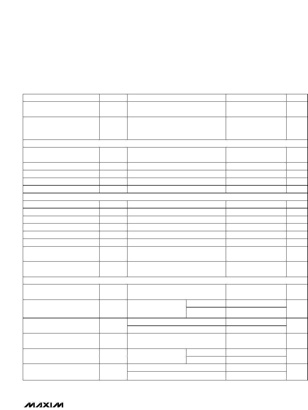
PARAMETER
SYMBOL
CONDITIONS
MIN TYP MAX
UNITS
POWER SUPPLY
MAX5058 4.5
28.0
Supply Voltage Range V+
MAX5059 9.3
28.0
V
Quiescent Supply Current I
Q
2.5 5 mA
MAX5058 4.5
Switching Supply Current I
SW
f
SW
= 250kHz at BUFIN
MAX5059 6
mA
I
REF
: REFERENCE CURRENT OUTPUT
Reference Current I
IREF
V
IREF
= 1.785V
49.2
50
51.1
µA
Reference Current Variation ΔI
IREF
V
IREF
= 0.5V to 2.5V
-0.1 +0.1
%/V
Reference Voltage Compliance
Range
Guaranteed by reference current variation
test
0.5 2.5 V
V
REG
: LOW-DROPOUT REGULATOR
MAX5058
4.75
5
5.25
Regulator Output V
VREG
I
VREG
= 0 to 30mA
MAX5059 9.4 10
10.6
V
MAX5058, V+ = 6V to 28V 25
Line Regulation
MAX5059, V+ = 11V to 28V 25
mV
MAX5058
V+
= 4.5V,
I
VREG
= 30mA
200
350
Dropout V
DROP
MAX5059
V+
= 9.3V,
I
VREG
= 30mA
200
350
mV
VP: INTERNAL REGULATOR
Regulator Output Setpoint V
VP
I
VP
= 0 to 5mA 3.8 4.3 V
ZC: ZERO-CURRENT COMPARATOR
Zero-Current Comparator
Threshold
V
ZCTH
T
A
= +25°C
+3.5
+5
+6.5
mV
Zero-Current Comparator Input
Current
I
ZC
-2.5 +2.5
µA
MAX5058/MAX5059
Parallelable Secondary-Side Synchronous Rectifier
Driver and Feedback-Generator Controller ICs
_______________________________________________________________________________________ 3
ELECTRICAL CHARACTERISTICS (continued)
(V+ = +12V, GND = PGND = 0, VDR = V
REG
, C
QSYNC
= C
QREC
= 0, ZCP = ZCN = BUFIN = CSP = CSN = SFN = VSN = GND, V
IREF
=
V
VSP
= 1.785V, C
VREG
= 2.2µF, C
VP
= 1µF, C
COMPS
= 0.1µF, C
SFP
= 68nF, T
A
= T
MIN
to T
MAX
, unless otherwise noted. Typical values
are at T
A
= +25°C.)
PARAMETER
SYMBOL
CONDITIONS
MIN
TYP
UNITS
Zero-Current Comparator Input
Range
V
ZC
-0.1 +1.5
V
Zero-Current Comparator
Propagation Delay
t
ZC
10mV overdrive, from when V
ZCP
- V
ZCN
is
greater than V
ZCTH
to when QSYNC goes
low
65 ns
BUFIN: SYNCHRONIZING PULSE INPUT
BUFIN to Output Propagation
Delay
t
pd
BUFIN rising to QREC rising or QSYNC
falling
40 ns
BUFIN Input Current I
BUFIN
-1 +1 µA
BUFIN Input Capacitance
C
BUFIN
10 pF
BUFIN Input-Logic High
V
HBUFIN
2.4 V
BUFIN Input-Logic Low
V
LBUFIN
0.8 V
MARGINING INPUTS
RMGD Resistance R
RMGD
Sinking 10mA 6.5 11 Ω
RMGU Resistance R
RMGU
Sinking 10mA 6.5 11 Ω
MRGD Input-Logic High
V
HMRGD
2.4 V
MRGD Input-Logic Low
V
LMRGD
0.8 V
MRGU Input-Logic High
V
HMRGU
2.4 V
MRGU Input-Logic Low
V
LMRGU
0.8 V
MRGU, MRGD Input Resistance
R
MRGD
,
R
MRGU
40 kΩ
RMGU, RMGD Leakage Current
I
RMGU
,
I
RMGD
-100 +100
nA
DRIVER OUTPUTS
QREC, QSYNC Peak Source
Current
I
QREC_SO,
I
QSYNC_SO
2A
MAX5058 75 150
QREC, QSYNC Output-Voltage
High
V
QREC_H,
V
QSYNC_H
Measured with respect to
V
VDR
, sourcing 50mA
MAX5059 75 150
mV
C
QREC
= C
QSYNC
= 0 30
QREC, QSYNC Low-to-High
Delay Time
t
PDLH
C
QREC
= C
QSYNC
= 5nF 70
ns
QREC, QSYNC Peak Sink Current
I
QREC_SI,
I
QSYNC_SI
2A
MAX5058 50 100
QREC, QSYNC Output-Voltage
Low
V
QREC_L,
V
QSYNC_L
Sinking 50mA
MAX5059 50 100
mV
C
QREC
= C
QSYNC
= 0 40
QREC, QSYNC High-to-Low
Delay Time
t
PDHL
C
QREC
= C
QSYNC
= 5nF 70
ns

MAX5058EUI+T

Mfr. #:
Manufacturer:
Maxim Integrated
Description:
Gate Drivers Secondary Side Synch Rectifier Driver
Lifecycle:
New from this manufacturer.
Delivery:
DHL FedEx Ups TNT EMS
Payment:
T/T Paypal Visa MoneyGram Western Union

Products related to this Datasheet