Reverse-Current Prevention
in Synchronous Rectifiers
One benefit of secondary-side synchronous rectifica-
tion is increased efficiency. Another benefit is that it
allows the inductor current to remain continuous
throughout the operating load range. This results in
constant loop dynamics that are easy to compensate.
In some cases, it may be necessary to turn off the free-
wheeling MOSFET when the current through this device
attempts to flow from drain to source. Turning off this
MOSFET can be done to enhance efficiency at low out-
put current. When multiple power supplies are paral-
leled, the power supply with the highest output voltage
has a tendency to source current into the power-supply
outputs with lower output voltage. Turning off the free-
wheeling MOSFET also prevents this current back-flow.
When the inductor current is allowed to become dis-
continuous, the loop dynamics change and the circuit
must be compensated accordingly to accommodate
stable continuous and discontinuous mode operation.
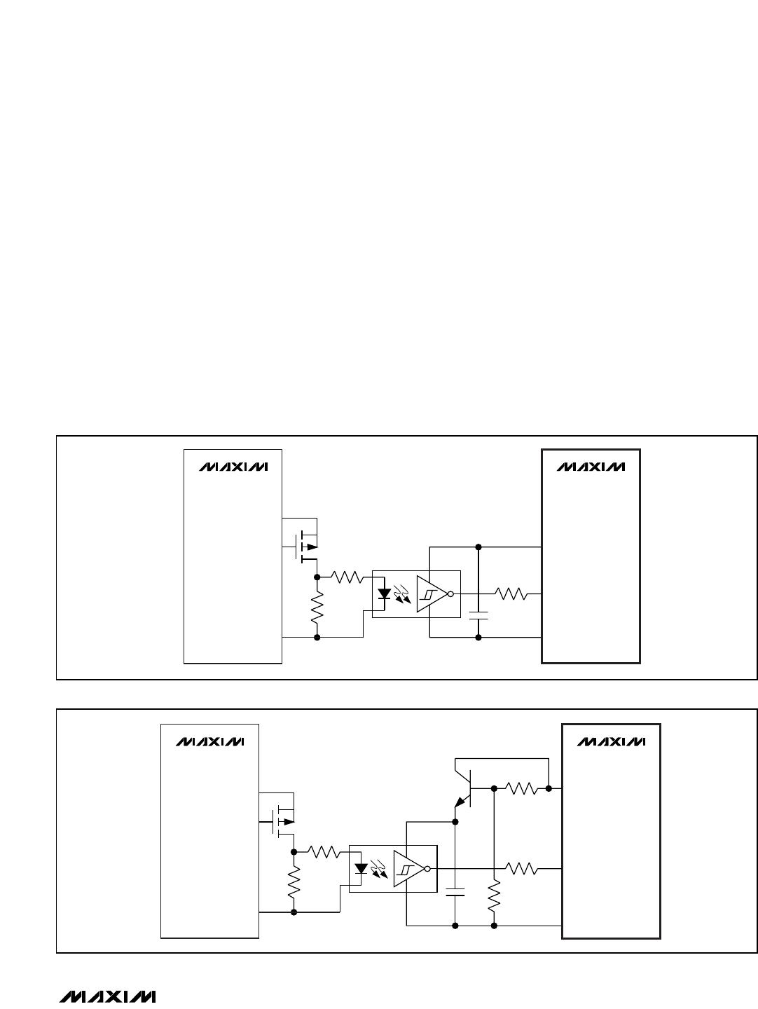
Turning off the freewheeling MOSFET is accomplished
by using the zero-current comparator (pins ZCP and
ZCN). Use this comparator to sense reverse current in
the freewheeling MOSFET and turn off the device by
pulling QSYNC low. An internal latch prevents the free-
wheeling MOSFET from turning on until the off-time of
the next cycle.
Reference Current
The MAX5058/MAX5059 do not have an explicit refer-
ence voltage generator. Instead, they contain a 1%-
accurate trimmed 50µA current source. This allows sig-
nificant flexibility in setting the reference voltage. In
some cases, the output-voltage resistive divider, con-
sisting of R1 and R2 in the Typical Application Circuit,
can be eliminated by selecting a suitable resistor value
at the I
REF
pin. This reduces the error that the output
voltage-divider may add. Use a low-value bypass
capacitance at this pin to eliminate noise. Typical values
for this capacitance are calculated by considering the
pole that it presents with R12. This pole must be placed
well beyond the frequency range of interest of the cur-
rent-share loop. Use values less than 2.2nF.
Error Amplifier
The MAX5058/MAX5059 incorporate a 1.3MHz unity
gain-bandwidth error amplifier with inputs INV, I
REF
,
and output COMPV. I
REF
is the noninverting input and
also serves as the reference voltage generator with the
internal 50µA current source and the external resistor
connected from I
REF
to GND. INV is the inverting input
and connects to the center of a resistive divider from
OUT to INV to GND. The output of the error amplifier,
COMPV, connects to the cathode of the LED in the
optocoupler to control the diode current that transmits
the error signal back to the primary-side controller. An
open-drain-output error amplifier simplifies interfacing
with the feedback optocoupler. Use this error amplifier
the same way as the industry-standard TL431 shunt ref-
erence. The open-drain output provides flexibility that
may be necessary when additional functionality such
as secondary current-limit regulation is required. Unlike
the TL431, the output of the internal error amplifier of
the MAX5058/MAX5059 is guaranteed to be a maxi-
mum of 200mV with a 5mA drain current, compared to
2.5V for the TL431 and 1.24V for the TLV431.
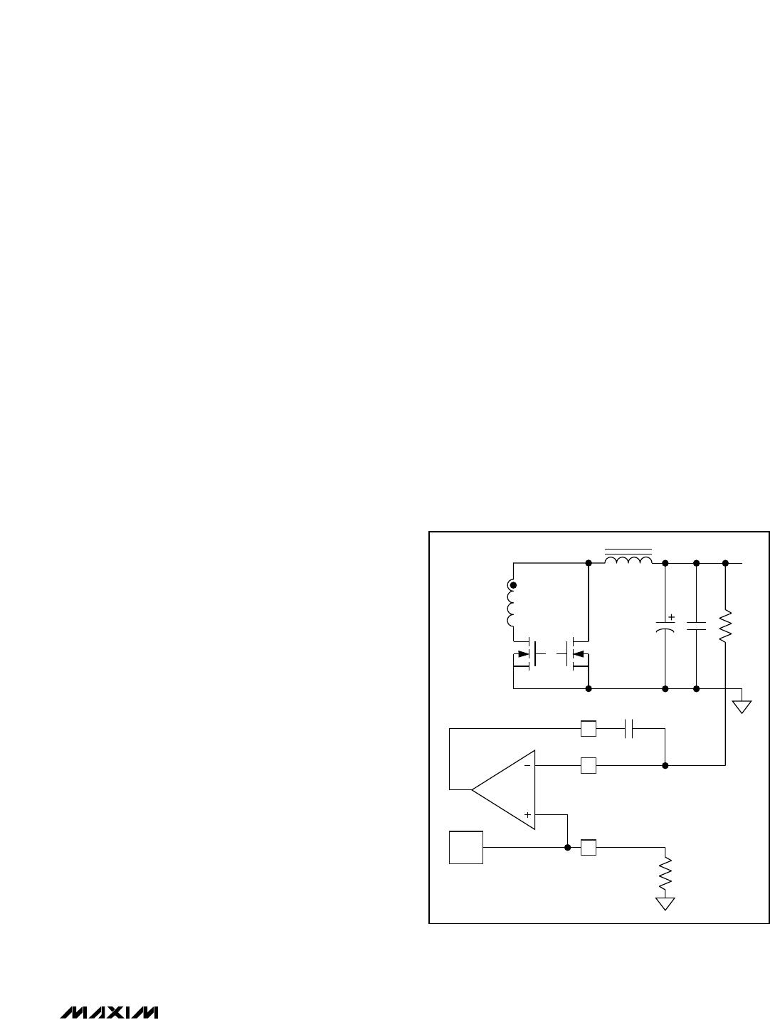
In some cases, it is possible to avoid the use of the out-
put voltage-divider (R1 and R2) by connecting INV to
the output through just R1. This eliminates the voltage
tolerance errors caused by R1 and R2. Output voltage
in this configuration is set directly by using a suitable
resistor at I
REF
. Figure 7 shows this configuration.
MAX5058/MAX5059
Parallelable Secondary-Side Synchronous Rectifier
Driver and Feedback-Generator Controller ICs
______________________________________________________________________________________ 15