MAX5058/MAX5059
Parallelable Secondary-Side Synchronous Rectifier
Driver and Feedback-Generator Controller ICs
12 ______________________________________________________________________________________
Detailed Description
The MAX5058/MAX5059 enable the design of high-effi-
ciency, isolated power supplies using synchronous rec-
tification on the secondary side. These devices
commutate the secondary-side MOSFETs by providing
a clean gate-drive signal that is synchronized to the
power MOSFET switching in the primary side of the iso-
lation transformer. Once fully enhanced, the secondary-
side MOSFETs have very low on-resistance, producing
a voltage drop much lower than Schottky diodes, result-
ing in much higher efficiencies. Simultaneous conduc-
tion of the synchronous rectifier MOSFETs is avoided by
having a look-ahead signal before the primary
MOSFETs turn on. This eliminates large current spikes
from a shorted transformer secondary.
The MAX5058 has a 5V internal gate-drive voltage reg-
ulator that can be used with logic-level MOSFETs. The
MAX5059 has a 10V internal gate-drive voltage regula-
tor that can be used with high-gate-voltage MOSFETs.
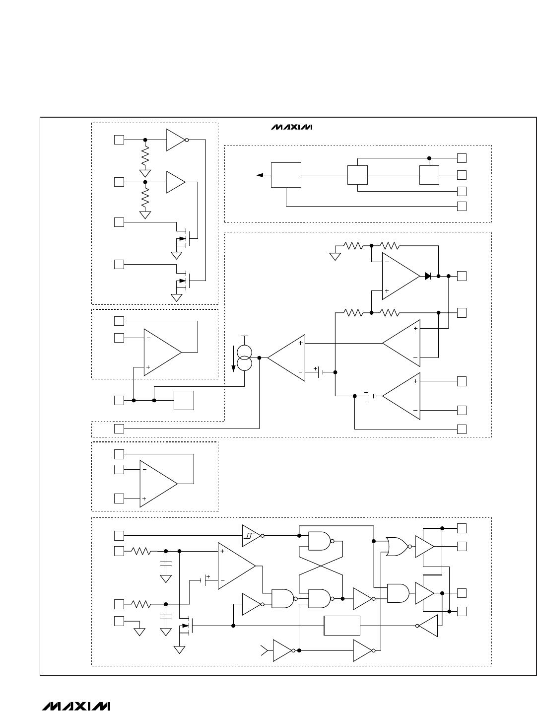
In addition to the gate drivers, there are blocks that
make the MAX5058/MAX5059 complete secondary-
side solutions. These blocks are as follows:
• Regulator and thermal-management block
• Buffer input and gate-driver block
• Reference-current block
• Error-amplifier block
• Margining block
• Remote-sense amplifier block
• Current-share block
Regulators and Thermal Management
The linear regulators in the MAX5058/MAX5059 provide
power for the internal circuitry, as well as power for run-
ning the external synchronous MOSFETs. Design is sim-
plified by deriving the power from the secondary
winding before the output-filter inductor. The peak volt-
age at the secondary is at least twice the output volt-
age, yielding more than 7V peak even for output
voltages down to 3.3V. Use a diode and a capacitor to
rectify and filter the voltage before applying it to V+ (see
D6 and C32 in the Typical Application Circuit). The
input for the regulator is V+ and the output is V
REG
.
Connect VDR to V
REG
to provide the supply for the gate
driver’s QREC and QSYNC. For logic-level MOSFETs,
use the MAX5058. For conventional MOSFETs that
require 10V to be fully enhanced, use the MAX5059.
The V+ input voltage range is from +4.5V to +28V.
Supply enough current to this input to satisfy the quies-
cent supply current of the MAX5058/MAX5059, as well
as the current for the MOSFET drivers. Estimate the total
required supply current by using the following formula:
where I
V+
is the current that must be supplied into V+
and Q
N3
, Q
N4
are the total gate charges of MOSFETs
N3 and N4 in the Typical Application Circuit. f
SW
is the
switching frequency and I
SW
is the switching current of
the part. Use high-quality ceramic capacitors to bypass
V+ and V
REG
. Use additional capacitance as required
for bypassing switching currents generated by the dri-
vers when driving the chosen MOSFETs. Connect at
least a 1µF ceramic capacitor at the output of the regu-
lator V
REG
for stability.
The MAX5058/MAX5059 have an exposed pad at the
back of the package to enable heatsinking directly to a
ground plane. When soldered to a 1in
2
copper island,
these devices are able to dissipate approximately 1.9W
at +70°C ambient temperature. Connect the exposed
pad to the GND.
In addition to the regulators, this block contains a ther-
mal-shutdown circuit that shuts down the gate drivers if
the die temperature exceeds +160°C. This is a last
resort shutdown mechanism. The trigger of this shut-
down mechanism must be avoided. Turning off the
secondary synchronous rectifier drivers in this manner
while the output carries the full load current causes the
current to be diverted to the lossy external diodes or
body diodes of the MOSFETs. This, in most cases,
leads to rectifier failure due to power dissipation. To
prevent this, make use of the TSF output (temperature
warning flag). TSF is an open-drain output that gets
asserted when the die temperature exceeds +125°C,
well before the actual thermal shutdown at +160°C. An
optocoupler connected from V
REG
to the TSF pin can
provide a means for shutting down the switching at the
primary side, thus avoiding catastrophic failure.
Buffer Input (BUFIN) and MOSFET Drivers
The MAX5058/MAX5059 drive external N-channel
MOSFETs at QSYNC and QREC. The QSYNC output
drives the gate of the freewheeling MOSFET N4 in the
Typical Application Circuit. The QREC output drives the
gate of the rectifying MOSFET N3 in the Typical
Application Circuit. Each gate-driver output is capable
of sinking and sourcing up to 2A peak current,
enabling the MAX5058/MAX5059 to drive high-gate-
charge MOSFETs.