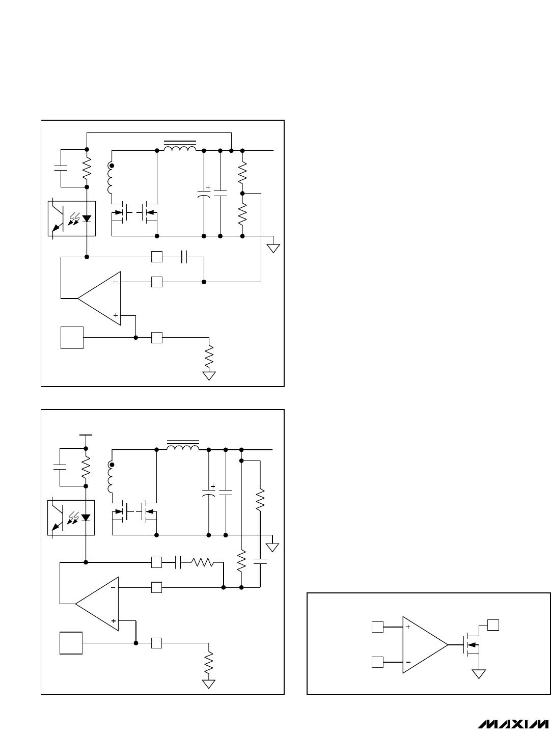
Figure 8 shows a typical configuration with output volt-
ages high enough (V
OUT
> 2.5V) to allow a typical
optocoupler to be fully biased. In this case, there are
two feedback paths—one though the error amplifier
and one through the output-connected optocoupler.
This second feedback path must be considered when
compensating the overall feedback loop.
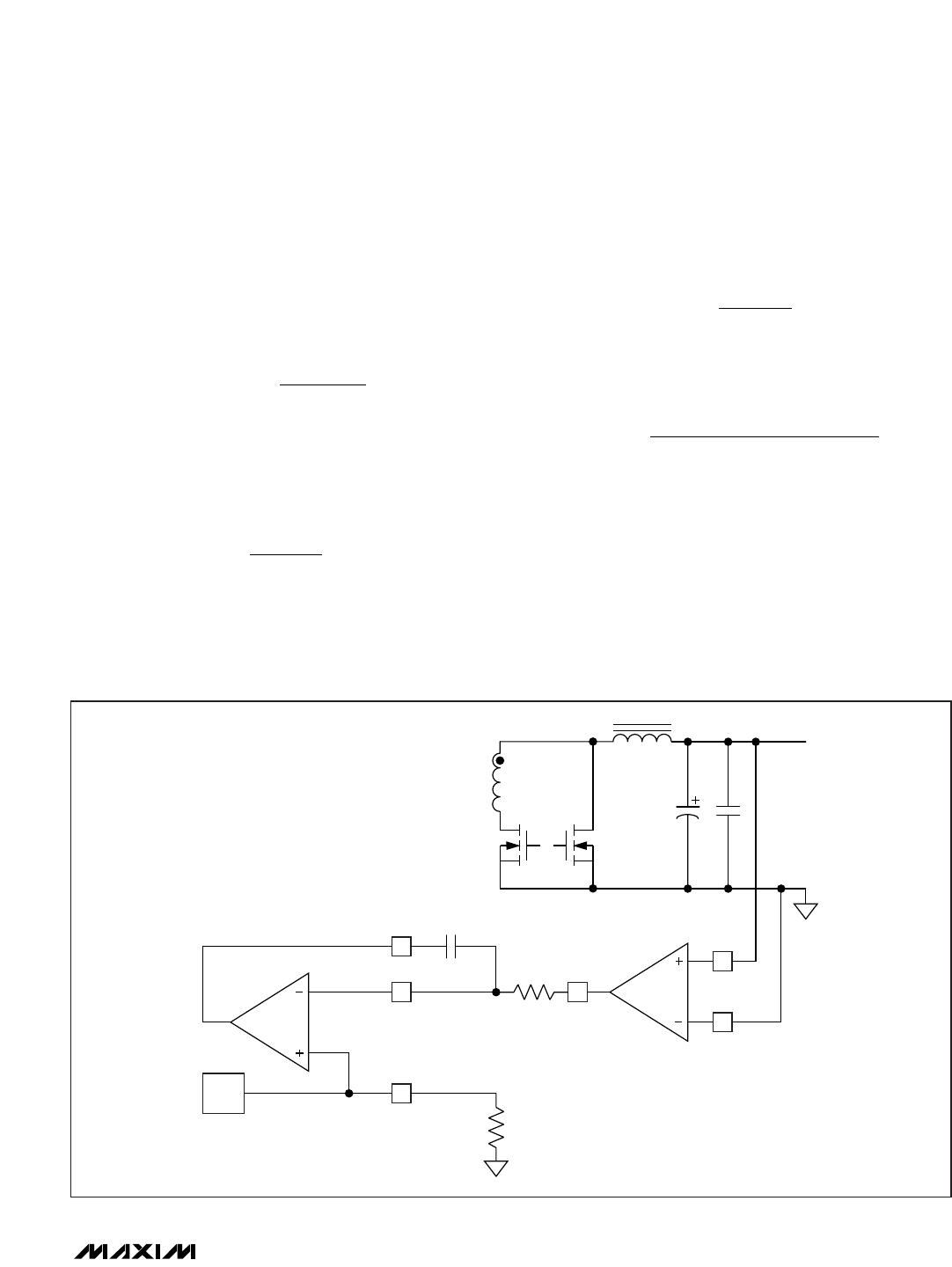
Figure 9 shows a typical configuration with an optocou-
pler for output voltages lower than 2.5V. In this case,
the direct connection of the optocoupler to the output is
not possible. There is only one feedback path and the
error-amplifier feedback network must be designed
accordingly.
Figure 10 shows the simplified block diagram for the
error amplifier.
Voltage Margining
The margining inputs MRGU (margin up) and MRGD
(margin down) control two internal MOSFETs with open-
drain outputs at RMGU and RMGD, respectively. When
margining is used, connect two pullup resistors from
RMGU and RMGD to I
REF
. A logic-high voltage at
MRGU causes QMU (see Figure 1) to open, increasing
the equivalent resistance at I
REF
and the reference volt-
age (V
IREF
). The error-amplifier inverting input, INV,
tracks I
REF
and forces the primary-side controller to
increase the output voltage. MRGD has the opposite
effect. When a logic high is applied to MRGD, QMD
turns on, decreasing the equivalent resistance at I
REF
and effectively reducing V
IREF
. This causes INV to track
and force the primary-side controller to reduce the out-
put voltage.
The margining inputs MRGU and MRGD are internally
pulled to GND with 40kΩ resistors. When margining is
not used, the inputs can be left floating or connected to
GND to make V
IREF
= 50µA × R12.
Calculation Procedure for Output-Voltage Setting
Resistors and Margining
Use the following step-by-step procedure to calculate
the output-voltage setting and margining resistors (see
the Typical Application Circuit):
MAX5058/MAX5059
Parallelable Secondary-Side Synchronous Rectifier
Driver and Feedback-Generator Controller ICs
16 ______________________________________________________________________________________
13
14
COMPV
INV
12
I
REF
E/A
I
REF
50μA
R12
V
OUT
> 2.5V
C28
R12
R12
R19
C27
Figure 8. Optocoupler Connection for V
OUT
> 2.5V
13
14
COMPV
INV
12
I
REF
E/A
I
REF
50μA
R12
0.5V < V
OUT
< 2.5V
C28
R1
Rff
R19
C27
Rf
Cf
V
REG
(PIN 23)
Figure 9. Optocoupler Connection for V
OUT
< 2.5V
13
COMPV
14
INV
12
I
REF
Figure 10. Simplified Error-Amplifier Diagram
MAX5058/MAX5059
Parallelable Secondary-Side Synchronous Rectifier
Driver and Feedback-Generator Controller ICs
______________________________________________________________________________________ 17
1) Select a parallel equivalent resistance R
eq
value to
produce the nominal reference voltage. For exam-
ple, R
eq
= 35.4kΩ gives you V
IREF
= 1.77V.
2) Select the margin-up percentage value:
ΔU = 5%
3) Calculate R
32
:
R
32
= 743.4kΩ. Calculated
Select the nearest 0.1% value.
R
32
= 741kΩ. Selected
4) Calculate R
12
:
R
12
= 37.05kΩ. Calculated
Select the nearest 0.1% value.
R
12
= 37kΩ. Selected
5) Select the margin-down percentage value:
ΔD = 5%
6) Recalculate R
eq
with the selected values:
R
eq
= 35.24kΩ.
7) Calculate R
33
:
R
33
= 361.186kΩ. Calculated
Select the nearest 0.1% value:
R
33
= 361kΩ. Selected
8) Calculate the reference voltage with the selected
chosen values:
V
IREF
= 50µA R
eq
.R
eq
from step 6.
V
IREF
= 1.762V.
R
RR
RDR
eq
eq
33
12
12
100
100 100
=
××
×+
()
×
%
%%Δ -
R
RR
RR
eq
=
+
12 32
12 32
R
RU
12
32
100
=
×
%
Δ
RR
U
U
eq32
100
+
% Δ
Δ
Figure 11. Remote-Sense Amplifier Connection for 0.5V V
OUT
2.5V
V
OUT
17
VSP
16
VSN
15
VSO
13
14
COMPV
INV
12
I
REF
E/A
I
REF
50μA
R12
C28
V
OUT
= (50μA) x R12
FOR: 0.5V V
OUT
2.5V
RSA
9) Select a value for R
1
and calculate R
2
for V
OUT
=
3.3V:
R
1
= 19.1kΩ
R
2
= 21.882kΩ.
Select the nearest 1% value.
R
2
= 21.8kΩ.
When margining is not used, substitute R
12
for R
eq
in step 8 and go to step 9.
Remote-Sense Amplifier
Use the remote-sense amplifier (RSA in Figure 1) to
directly sense the voltage across the load, compensat-
ing for voltage drops in PC board tracks or load con-
nection wires. The remote-sense amplifier is a
unity-gain amplifier with sufficient bandwidth to not
interfere with the normal operation of the voltage-con-
trol loop. Direct sensing of the output voltage is possi-
ble if the output voltage is between 0.5V to 2.5V. Figure
11 shows this configuration. Figure 12 shows the use of
the remote-sense amplifier with a voltage-divider. The
remote-sense amplifier has an input bias current of
100µA. The impedance of R1 and R2 must be kept low
in this configuration to avoid excessive errors in the out-
put-voltage set point.
Current Sharing
When multiple power modules are providing power to
the same load, the load current must be shared equally
to provide the best reliability and thermal distribution.
The MAX5058/MAX5059 contain circuitry that enable
current sharing among paralleled power supplies with-
out requiring an explicit controlling master circuit.
Current sharing is accomplished by connecting togeth-
er the current-share bus pins (SFP and SFN) of all par-
alleled power supplies (see Figure 13), thus creating a
current-force/share bus. The voltage level on this differ-
ential bus is proportional to the output current of the
power supply that has the highest current compared to
the other supplies. The number of power supplies that
can be paralleled with this method is limited only by
practical considerations.
R
V
VV
R
IREF
OUT IREF
2
1=
-
MAX5058/MAX5059
Parallelable Secondary-Side Synchronous Rectifier
Driver and Feedback-Generator Controller ICs
18 ______________________________________________________________________________________
Figure 12. Remote-Sense Amplifier Connection for V
OUT
> 2.5V (or any Other Arbitrary Voltage)
V
OUT
17
VSP
16
VSN
15
VSO
RSA
13
14
COMPV
V
OUT
= 1 +
V
IREF
V
IREF
= (
50μA
)
R12
R1
R2
INV
12
I
REF
E/A
I
REF
50μA
R12
C28
R2
R1
( )

MAX5058EUI+T

Mfr. #:
Manufacturer:
Maxim Integrated
Description:
Gate Drivers Secondary Side Synch Rectifier Driver
Lifecycle:
New from this manufacturer.
Delivery:
DHL FedEx Ups TNT EMS
Payment:
T/T Paypal Visa MoneyGram Western Union

Products related to this Datasheet