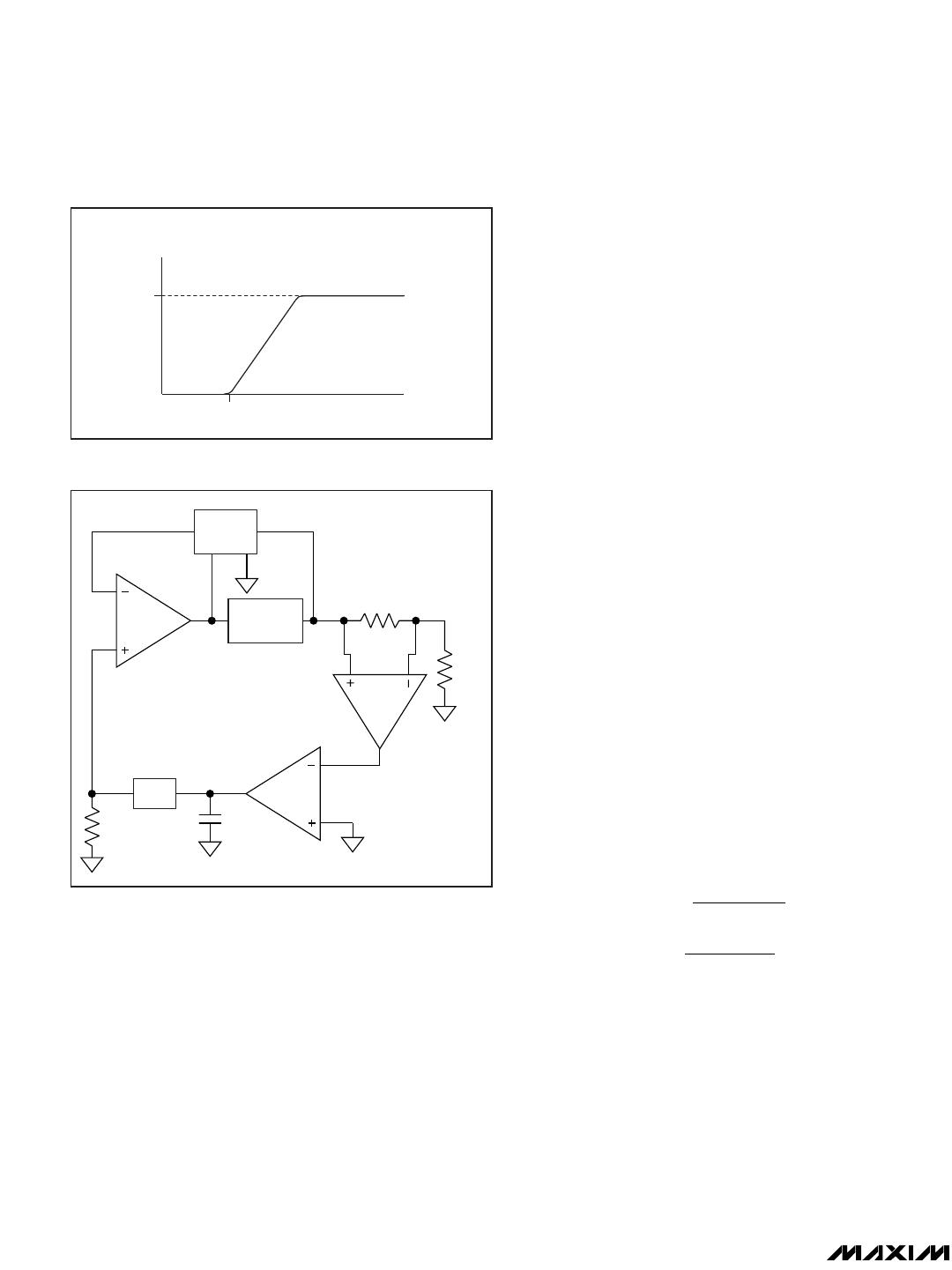
The adjustment range and thus the sharing capability of
the modules is limited by the amount of additional out-
put voltage boost possible through the VtoI block. The
typical voltage boost is +3% (i.e., 1.5µA/50µA). Figure
14 shows the transfer function of the VtoI block. This
adjustment range also sets a limit on the amount of volt-
age drop allowed for current sharing. For effective cur-
rent sharing, the sum of all voltage drops must be kept
below 3% and the output-to-load connection drop of
each power module must be kept equal.
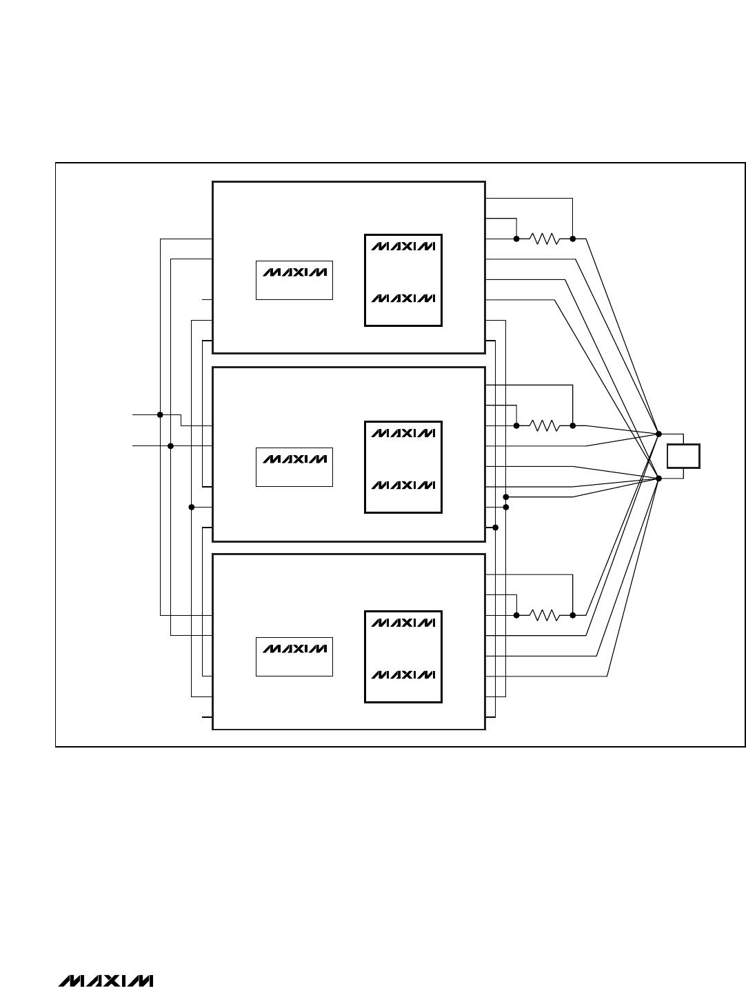
Current-sharing functions follow:
The voltage across the current-sense resistor for each
module is sensed and compared to the voltage on the
current-share bus. The voltage on the current-share bus
represents the current from the module that has the high-
est output current compared to the other modules. Each
module compares its current to this maximum current. If
its current is less than the maximum, then the module
increases its reference current with the VtoI block. This
raises the reference voltage presented at the noninvert-
ing input of the error amplifier. With a higher reference
voltage, the output voltage of the module rises in an
attempt to increase its output current. This process con-
tinues until the currents balance between the modules.
The current-adjust amplifier (see Figure 1) has an offset
at its inverting input that requires the share-bus voltage
to reach 40mV before the current-share control loop
attempts to regulate the output-load-current balance.
Thus, the current-share regulation does not begin until
the current-sense signals have exceeded 2mV (i.e.,
42mV/20).
Figure 15 shows the simplified equivalent small-signal
circuit of the current-share control loop. The current-
adjust amplifier represents the error amplifier in this
loop. The command signal, which is the voltage across
the SFP and SFN pins, is applied to the noninverting
input of this amplifier. For small-signal analysis, the
noninverting pin is shown grounded in Figure 15. This is
a low-bandwidth loop.
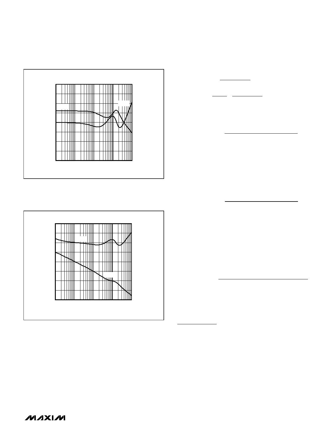
Assuming a much smaller unity-gain crossover bandwidth
(f
CS
) for the current-share loop compared to the main out-
put-voltage-regulation loop (i.e., f
CS
<< f
C
), the open-loop
gain of the current-share loop can be written as:
where f
CS
is the unity-gain crossover frequency of the
current-share loop (typically 10Hz to 100Hz), f
C
is the
unity-gain crossover frequency of the main output loop,
G
PS
(s) is the gain of the power stage from the refer-
ence voltage input of the error amplifier to the output
(G
PS
= V
OUT
/V
IREF
), R
S
is the current-sense resistor,
and R
LOAD
is the load resistance. Note that the current-
share loop bandwidth is highest for the lowest value of
R
LOAD
(maximum load).