Buffered 2:1 TMDS Switch
with Equalization
AD8194
Rev. 0
Information furnished by Analog Devices is believed to be accurate and reliable. However, no
responsibility is assumed by Analog Devices for its use, nor for any infringements of patents or other
rights of third parties that may result from its use. Specifications subject to change without notice. No
license is granted by implication or otherwise under any patent or patent rights of Analog Devices.
Trademarks and registered trademarks are the property of their respective owners.
One Technology Way, P.O. Box 9106, Norwood, MA 02062-9106, U.S.A.
Tel: 781.329.4700 www.analog.com
Fax: 781.461.3113 ©2007 Analog Devices, Inc. All rights reserved.
FEATURES
2 inputs, 1 output HDMI/DVI high speed signal switch
Pin-to-pin compatible with the AD8193
Enables HDMI 1.3-compliant receiver
4 TMDS channels per input/output
Supports 250 Mbps to 2.25 Gbps data rates
Supports 25 MHz to 225 MHz pixel clocks
Fully buffered unidirectional inputs/outputs
Equalized inputs for operation with long HDMI cables
(20 m at 2.25 Gbps)
Matched 50 Ω input and output on-chip terminations
Low added jitter
Single-supply operation (3.3 V)
Standards compliant: HDMI receiver, DVI
32-lead, 5 mm × 5 mm, RoHS-compliant LFCSP
APPLICATIONS
Advanced television (HDTV) sets
Multiple input displays
Projectors
A/V receivers
Set-top boxes
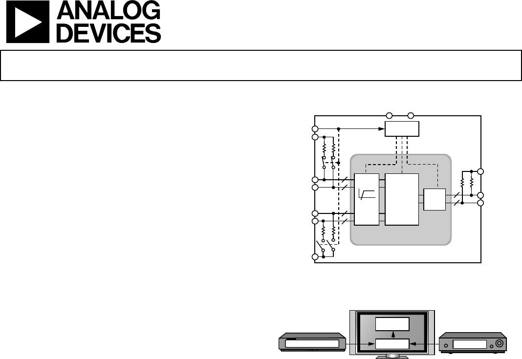
FUNCTIONAL BLOCK DIAGRAM
07004-001
AD8194
CONTROL
LOGIC
+4
4
+
+
4
4
4
4
Tx
SWITCH
CORE
HIGH SPEED BUFFERED
VTTO
VTTI
IP_A[3:0]
IN_A[3:0]
IP_B[3:0]
IN_B[3:0]
VTTI
S_SEL
OP[3:0]
ON[3:0]
A
V
C
C
A
V
EE
EQ
Figure 1.
TYPICAL APPLICATION
HDMI
RECEIVER
AD8194
HDTV SET
DVD PLAYER
SET-TOP BOX
07004-002
Figure 2. Typical AD8194 Application for HDTV Sets
GENERAL DESCRIPTION
The AD8194 is a low cost quad 2:1 TMDS® switch for high
speed HDMI™/DVI video applications. The AD8194 features
equalized inputs, ideal for systems with long cable runs. Its
primary function is to switch the high speed signals from one
of two single-link (HDMI or DVI) sources to the single-link
output. The AD8194 is a fully buffered switch solution with 50
input and output terminations, providing full-swing output
signal recovery and minimizing reflections for improved system
signal integrity.
The AD8194 is provided in a space-saving, 32-lead, LFCSP,
surface-mount, RoHS-compliant, plastic package and is specified
to operate over the −40°C to +85°C temperature range.
PRODUCT HIGHLIGHTS
1. Data supports rates up to 2.25 Gbps, enabling greater than
1080p deep color (12-bit color) HDMI formats and greater
than UXGA (1600 × 2300) DVI resolutions.
2. Fully buffered inputs and outputs.
3. Input cable equalizer enables use of long cables at the
input. For a typical 24 AWG cable, the AD8194 compen-
sates for more than 20 m at data rates up to 2.25 Gbps.
4. Matched 50 Ω on-chip input and output terminations
improve system signal integrity.
5. Single-pin source select bit.
6. Low added jitter.
AD8194* PRODUCT PAGE QUICK LINKS
Last Content Update: 02/23/2017
COMPARABLE PARTS
View a parametric search of comparable parts.
EVALUATION KITS
AD8194 Evaluation Board
DOCUMENTATION
Data Sheet
AD8194: Buffered 2:1 TMDS Switch with Equalization Data
Sheet
REFERENCE MATERIALS
Informational
Advantiv™ Advanced TV Solutions
Technical Articles
Analysis of Common Failures of HDMI CT
DESIGN RESOURCES
AD8194 Material Declaration
PCN-PDN Information
Quality And Reliability
Symbols and Footprints
DISCUSSIONS
View all AD8194 EngineerZone Discussions.
SAMPLE AND BUY
Visit the product page to see pricing options.
TECHNICAL SUPPORT
Submit a technical question or find your regional support
number.
DOCUMENT FEEDBACK
Submit feedback for this data sheet.
This page is dynamically generated by Analog Devices, Inc., and inserted into this data sheet. A dynamic change to the content on this page will not
trigger a change to either the revision number or the content of the product data sheet. This dynamic page may be frequently modified.
AD8194
Rev. 0 | Page 2 of 16
TABLE OF CONTENTS
Features .............................................................................................. 1
Applications....................................................................................... 1
Functional Block Diagram .............................................................. 1
Typical Application........................................................................... 1
General Description......................................................................... 1
Product Highlights ........................................................................... 1
Revision History ............................................................................... 2
Specifications..................................................................................... 3
Absolute Maximum Ratings............................................................ 4
Thermal Resistance ...................................................................... 4
Maximum Power Dissipation ..................................................... 4
ESD Caution.................................................................................. 4
Pin Configuration and Function Descriptions............................. 5
Typical Performance Characteristics ..............................................6
Theory of Operation .........................................................................9
Introduction...................................................................................9
Input Channels ..............................................................................9
Output Channels ...........................................................................9
Switching Mode.......................................................................... 10
Application Notes........................................................................... 11
Switching High Speed Signals................................................... 11
Switching Low Speed Signals.................................................... 11
PCB Layout Guidelines.............................................................. 11
Outline Dimensions ....................................................................... 16
Ordering Guide .......................................................................... 16
REVISION HISTORY
11/07—Revision 0: Initial Version

AD8194ACPZ

Mfr. #:
Manufacturer:
Analog Devices Inc.
Description:
Equalizers 2:1 TMDS Switch Buffered w/ Equal
Lifecycle:
New from this manufacturer.
Delivery:
DHL FedEx Ups TNT EMS
Payment:
T/T Paypal Visa MoneyGram Western Union

Products related to this Datasheet