AD8194
Rev. 0 | Page 11 of 16
APPLICATION NOTES
SWITCHING HIGH SPEED SIGNALS
The AD8194 is a quad 2:1 TMDS switch that is used to switch
the high speed signals of two input HDMI links to a single
HDMI output.
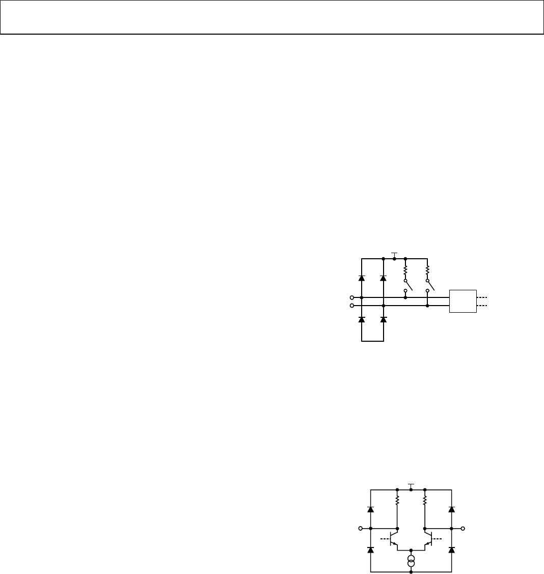
SWITCHING LOW SPEED SIGNALS
Because the AD8194 is a TMDS-only switch, a complete HDMI
switch solution requires another component to switch the low
speed DDC channels.
The HDMI 1.3 specification places a number of restrictions on
the low speed signal path that limit the selection of a suitable
low cost DDC switch. The first requirement is that the switch
must be bidirectional to convey the I
2
C® protocol signals that
pass through it. A CMOS device is the simplest switch with this
capability.
The second HDMI requirement for the DDC signals is that the
total DDC signal path capacitance be less than 50 pF. The total
capacitance comprises the HDMI connector, the PC board
traces, the DDC switch, and the input capacitance of the HDMI
receiver. As a practical design consideration, a suitable DDC
switch has a total channel capacitance of less than 10 pF.
Finally, the channel on-resistance (R
ON
) of the DDC switch must
not be too high; otherwise, the voltage drop across it violates
the maximum V
OL
of the I
2
C signals. Any switch with an on
resistance of approximately 100 is sufficient in a typical
application, assuming that the end application includes an
I
2
C-compliant receiver device. Switches with lower channel
on resistance have improved V
OL
performance.
For the AD8194 evaluation board, the MC74LVX4053 was
chosen to switch the low speed signals. This part has a maximum
R
ON
of 108 and a maximum parasitic capacitance of 10 pF.
Refer to the
Evaluation Board section for details on how to use
the MC74LVX4053 with the AD8194 in an application.
PCB LAYOUT GUIDELINES
The AD8194 is used to switch HDMI/DVI video signals, which
are differential, unidirectional, and high speed (up to 2.25 Gbps).
The channels that carry the video data must be controlled
impedance, terminated at the receiver, and capable of operating
up to at least 2.25 Gbps. It is especially important to note that
the differential traces that carry the TMDS signals should be
designed with a controlled differential impedance of 100 Ω.
The AD8194 provides single-ended 50 Ω terminations on chip
for both its inputs and outputs. Transmitter termination is not
fully specified by the HDMI standard, but the inclusion of the
50 Ω output terminations improves the overall system signal
integrity.
TMDS Signals
The audiovisual (AV) data carried on these high speed channels
is encoded by a technique called Transition Minimized Differ-
ential Signaling (TMDS) and, in the case of HDMI, is also
encrypted according to the high bandwidth digital content
protection (HDCP) standard.
In the HDMI/DVI standard, four differential pairs carry the
TMDS signals. For DVI, three of these pairs are dedicated to
carrying RGB video and sync data. For HDMI, audio data is
also interleaved with the video data; the DVI standard does
not incorporate audio information. The fourth high speed
differential pair is used for the AV data-word clock and runs
at one-tenth the speed of the TMDS data channels.
The four high speed channels of the AD8194 are identical.
No concession was made to lower the bandwidth of the fourth
channel for the pixel clock, so any channel can be used for any
TMDS signal. The user chooses which signal is routed over
which channel. Additionally, the TMDS channels are symmetrical;
therefore, the p and n of a given differential pair are inter-
changeable, provided the inversion is consistent across all inputs
and outputs of the AD8194. However, the routing between
inputs and outputs through the AD8194 is fixed. For example,
Output Channel 0 always switches between Input A0 and
Input B0, and so forth.
The AD8194 buffers the TMDS signals, and the input traces can
be considered electrically independent of the output traces. In
most applications, the quality of the signal on the input TMDS
traces is more sensitive to the PCB layout. Regardless of the
data being carried on a specific TMDS channel, or whether the
TMDS line is at the input or the output of the AD8194, all four
high speed signals should be routed on a PCB in accordance
with the same RF layout guidelines.
Layout for the TMDS Signals
The TMDS differential pairs can be either microstrip traces,
routed on the outer layer of a board, or stripline traces, routed
on an internal layer of the board. If microstrip traces are used,
there should be a continuous reference plane on the PCB layer
directly below the traces. If stripline traces are used, they must
be sandwiched between two continuous reference planes in the
PCB stackup. Additionally, the p and n of each differential pair
must have a controlled differential impedance of 100 Ω. The
characteristic impedance of a differential pair is a function of
several variables, including the trace width, the distance separating
the two traces, the spacing between the traces and the reference
plane, and the dielectric constant of the PC board binder material.
Interlayer vias introduce impedance discontinuities that can
cause reflections and jitter on the signal path; therefore, it is
preferable to route the TMDS lines exclusively on one layer of the
board, particularly for the input traces. Additionally, to prevent
unwanted signal coupling and interference, route the TMDS
signals away from other signals and noise sources on the PCB.