AD8194
Rev. 0 | Page 3 of 16
SPECIFICATIONS
T
A
= 27°C, AVCC = 3.3 V, VTTI = 3.3 V, VTTO = 3.3 V, AVEE = 0 V, differential input swing = 1000 mV, pattern = PRBS 2
7
− 1,
data rate = 2.25 Gbps, TMDS outputs terminated with external 50 Ω resistors to 3.3 V, unless otherwise noted.
Table 1.
Parameter Conditions/Comments Min Typ Max Unit
DYNAMIC PERFORMANCE
Maximum Data Rate (DR) per Channel NRZ 2.25 Gbps
Bit Error Rate (BER) 10
−9
Added Deterministic Jitter 10 ps (p-p)
Added Random Jitter 1 ps (rms)
Differential Intrapair Skew At output 1 ps
Differential Interpair Skew
1
At output 30 ps
EQUALIZATION PERFORMANCE
Receiver Boost frequency = 1.125 GHz 12 dB
INPUT CHARACTERISTICS
Input Voltage Swing Differential 150 1200 mV
Input Common-Mode Voltage (V
ICM
) AVCC − 800 AVCC mV
OUTPUT CHARACTERISTICS
High Voltage Level Single-ended high speed channel AVCC mV
Low Voltage Level Single-ended high speed channel AVCC − 600 AVCC − 400 mV
Rise/Fall Time (20% to 80%) 75 178 ps
TERMINATION
Input Resistance Single-ended 50 Ω
Output Resistance Single-ended 50 Ω
POWER SUPPLY
AVCC Operating range 3 3.3 3.6 V
QUIESCENT CURRENT
2
AVCC 50 70 mA
VTTI 40 54 mA
VTTO 40 65 mA
POWER DISSIPATION
3
429 mW
SOURCE SELECT INTERFACE
Input High Voltage (V
IH
) S_SEL 2 V
Input Low Voltage (V
IL
) S_SEL 0.8 V
1
Differential interpair skew is measured between the TMDS pairs of a single link.
2
Typical value assumes only the selected HDMI/DVI link is active with nominal signal swings and that the unselected HDMI/DVI link is deactivated. Minimum and
maximum limits are measured at the respective extremes of input termination resistance and input voltage swing.
3
The total power dissipation excludes power dissipated in the 50 Ω off-chip loads.
AD8194
Rev. 0 | Page 4 of 16
ABSOLUTE MAXIMUM RATINGS
Table 2.
Parameter Rating
AVCC to AVEE 3.7 V
VTTI AVCC + 0.6 V
VTTO AVCC + 0.6 V
Internal Power Dissipation 1.2 W
High Speed Input Voltage AVCC − 1.4 V < V
IN
< AVCC + 0.6 V
High Speed Differential
Input Voltage
2.0 V
Source Select (S_SEL) AVEE − 0.3 V < V
IN
< AVCC + 0.6 V
Storage Temperature Range −65°C to +125°C
Operating Temperature
Range
−40°C to +85°C
Junction Temperature 150°C
Stresses above those listed under Absolute Maximum Ratings
may cause permanent damage to the device. This is a stress
rating only; functional operation of the device at these or any
other conditions above those indicated in the operational
section of this specification is not implied. Exposure to absolute
maximum rating conditions for extended periods may affect
device reliability.
THERMAL RESISTANCE
θ
JA
is specified for the worst-case conditions: a device soldered
in a 4-layer JEDEC circuit board for surface-mount packages.
θ
JC
is specified for the exposed pad soldered to the circuit board
with no airflow.
Table 3. Thermal Resistance
Package Type
θ
JA
θ
JC
Unit
32-Lead LFCSP 47 6.8 °C/W
MAXIMUM POWER DISSIPATION
The maximum power that can be safely dissipated by the
AD8194 is limited by the associated rise in junction tempera-
ture. The maximum safe junction temperature for plastic
encapsulated devices is determined by the glass transition
temperature of the plastic, approximately 150°C. Temporarily
exceeding this limit may cause a shift in parametric performance
due to a change in the stresses exerted on the die by the package.
Exceeding a junction temperature of 175°C for an extended
period can result in device failure. To ensure proper operation,
it is necessary to observe the maximum power derating as
determined by the coefficients in
Table 3.
ESD CAUTION
AD8194
Rev. 0 | Page 5 of 16
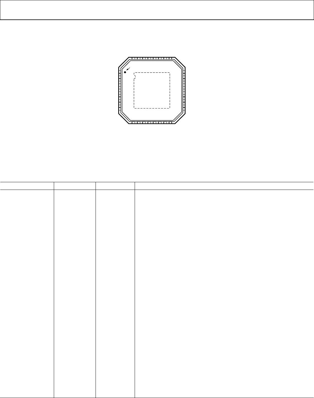
PIN CONFIGURATION AND FUNCTION DESCRIPTIONS
1
2
3
4
5
6
7
8
IN_A2
IP_A2
VTTI
IN_A3
IP_A3
AVCC
OP3
ON3
32
31
30
29
28
27
26
25
9
10
11
12
13
14
15
16
OP2
ON2
AVEE
OP1
ON1
VTTO
OP0
ON0
IP_B2
IN_B2
AVCC
IP_B1
IN_B1
VTTI
IP_B0
IN_B0
24
23
22
21
20
19
18
17
PIN 1
INDICATOR
IP_A1
IN_A1
S_SEL
IP_A0
IN_A0
AVEE
IP_B3
IN_B3
AD8194
TOP VIEW
(Not to Scale)
07004-003
NOTES
1. THE AD8194 LFCSP HAS AN EXPOSED PADDLE (ePAD) ON THE UNDERSIDE
OF THE PACKAGE, WHICH AIDS IN HEAT DISSIPATION. THE ePAD MUST BE
ELECTRICALLY CONNECTED TO THE AVEE SUPPLY PLANE TO MEET
THERMAL SPECIFICATIONS.
Figure 3. Pin Configuration
Table 4. Pin Function Descriptions
Pin No. Mnemonic Type
1
Description
1 IN_A2 HS I High Speed Input Complement.
2 IP_A2 HS I High Speed Input.
3, 19 VTTI Power Input Termination Supply. Nominally connected to AVCC.
4 IN_A3 HS I High Speed Input Complement.
5 IP_A3 HS I High Speed Input.
6, 22 AVCC Power Positive Power Supply. 3.3 V nominal.
7 OP3 HS O High Speed Output.
8 ON3 HS O High Speed Output Complement.
9 OP2 HS O High Speed Output.
10 ON2 HS O High Speed Output Complement.
11, 27, ePAD AVEE Power Negative Power Supply. 0 V nominal.
12 OP1 HS O High Speed Output.
13 ON1 HS O High Speed Output Complement.
14 VTTO Power Output Termination Supply. Nominally connected to AVCC.
15 OP0 HS O High Speed Output.
16 ON0 HS O High Speed Output Complement.
17 IN_B0 HS I High Speed Input Complement.
18 IP_B0 HS I High Speed Input.
20 IN_B1 HS I High Speed Input Complement.
21 IP_B1 HS I High Speed Input.
23 IN_B2 HS I High Speed Input Complement.
24 IP_B2 HS I High Speed Input.
25 IN_B3 HS I High Speed Input Complement.
26 IP_B3 HS I High Speed Input.
28 IN_A0 HS I High Speed Input Complement.
29 IP_A0 HS I High Speed Input.
30 S_SEL Control Source Selector Pin.
31 IN_A1 HS I High Speed Input Complement.
32 IP_A1 HS I High Speed Input.
1
HS = high speed, I = input, O = output.

AD8194ACPZ

Mfr. #:
Manufacturer:
Analog Devices Inc.
Description:
Equalizers 2:1 TMDS Switch Buffered w/ Equal
Lifecycle:
New from this manufacturer.
Delivery:
DHL FedEx Ups TNT EMS
Payment:
T/T Paypal Visa MoneyGram Western Union

Products related to this Datasheet