AD8194
Rev. 0 | Page 12 of 16
Both traces of a given differential pair must be equal in length
to minimize intrapair skew. Maintaining the physical symmetry
of a differential pair is integral to ensuring its signal integrity;
excessive intrapair skew can introduce jitter through duty
cycle distortion (DCD). The p and n of a given differential pair
should always be routed together to establish the required 100 Ω
differential impedance. Enough space should be left between
the differential pairs of a given group so that the n of one pair
does not couple to the p of another pair. For example, one tech-
nique is to make the interpair distance 4 to 10 times wider than
the intrapair spacing.
Any group of four TMDS channels (Input A, Input B, or the
output) should have closely matched trace lengths to minimize
interpair skew. Severe interpair skew can cause the data on the
four different channels of a group to arrive out of alignment
with one another. A good practice is to match the trace lengths
for a given group of four channels to within 0.05 inches on FR4
material.
The length of the TMDS traces should be minimized to reduce
overall signal degradation. Commonly used PC board material
such as FR4 is lossy at high frequencies; therefore, long traces
on the circuit board increase signal attenuation, resulting in
decreased signal swing and increased jitter through intersymbol
interference (ISI).
Controlling the Characteristic Impedance of a TMDS
Differential Pair
The characteristic impedance of a differential pair depends on a
number of variables, including the trace width, the distance
between the two traces, the height of the dielectric material
between the trace and the reference plane below it, and the
dielectric constant of the PCB binder material. To a lesser
extent, the characteristic impedance also depends upon the
trace thickness and the presence of solder mask.
There are many combinations that can produce the correct
characteristic impedance. It is generally required to work with
the PC board fabricator to obtain a set of parameters to produce
the desired results.
To guarantee a differential pair with a differential impedance of
100 Ω over the entire length of the trace, change the width of
the traces in a differential pair based on how closely one trace is
coupled to the other. When the two traces of a differential pair
are close and strongly coupled, they should have a width that
produces a 100 Ω differential impedance. When the traces split
apart to go into a connector, for example, and are no longer so
strongly coupled, the width of the traces should be increased to
yield a differential impedance of 100 Ω in the new configuration.
Ground Current Return
In some applications, it may be necessary to invert the output
pin order of the AD8194. This requires routing the TMDS
traces on multiple layers of the PCB. When routing differential
pairs on multiple layers, it is also necessary to reroute the
corresponding reference plane to provide one continuous
ground current return path for the differential signals. Standard
plated through-hole vias are acceptable for both the TMDS
traces and the reference plane. An example of this is illustrated
in
Figure 21.
PCB DIELECTRIC
SILKSCREEN
SILKSCREEN
PCB DIELECTRIC
PCB DIELECTRIC
LAYER 2: GND (REFERENCE PLANE)
LAYER 4: SIGNAL (MICROSTRIP)
THROUGH-HOLE VIAS
LAYER 1: SIGNAL (MICROSTRIP)
KEEP REFERENCE PLANE
ADJACENT TO SIGNAL ON ALL
LAYERS TO PROVIDE CONTINUOUS
GROUND CURRENT RETURN PATH.
LAYER 3: PWR
(REFERENCE PLANE)
07004-012
Figure 21. Example Routing of Reference Plane
TMDS Terminations
The AD8194 provides internal 50 Ω single-ended terminations
for all of its high speed inputs and outputs. The termination
resistors back-terminate the output TMDS transmission lines.
These back-terminations act to absorb reflections from imped-
ance discontinuities on the output traces, improving the signal
integrity of the output traces and adding flexibility to how the
output traces can be routed. For example, interlayer vias can be
used to route the AD8194 TMDS outputs on multiple layers of the
PCB without severely degrading the quality of the output signal.
In a typical application, the AD8194 output is connected to an
HDMI/DVI receiver or to another device with a 50 Ω single-ended
input termination. It is recommended that the outputs be
terminated with external 50 Ω on-board resistors when the
AD8194 is not connected to another device.
AD8194
Rev. 0 | Page 13 of 16
Auxiliary Control Signals
There are four single-ended control signals associated with each
source or sink in an HDMI/DVI application. These are hot plug
detect (HPD), consumer electronics control (CEC), and two
display data channel (DDC) lines. The two signals on the DDC
bus are SDA and SCL (serial data and serial clock, respectively).
The AD8194, which is a low cost part, does not have any addi-
tional capability to switch these signals; other means are
required to switch these signals if required.
In general, it is sufficient to route each auxiliary signal as a
single-ended trace. These signals are not sensitive to impedance
discontinuities, do not require a reference plane, and can be
routed on multiple layers of the PCB. However, it is best to
follow strict layout practices whenever possible to prevent the
PCB design from affecting the overall application. The specific
routing of the HPD, CEC, and DDC lines depends upon the
application in which the AD8194 is being used.
For example, the maximum speed of signals present on the
auxiliary lines is 100 kHz I
2
C data on the DDC lines; therefore,
any layout that enables 100 kHz I
2
C to be passed over the DDC
bus should suffice. The HDMI 1.3 specification, however, places
a strict 50 pF limit on the amount of capacitance that can be
measured on either SDA or SCL at the HDMI input connector.
This 50 pF limit includes the HDMI connector, the PCB, the
capacitance of the CMOS switch, and whatever capacitance is
seen at the input of the HDMI receiver. There is a similar limit
of 100 pF of input capacitance for the CEC line.
The parasitic capacitance of traces on a PCB increases with
trace length. To help ensure that a design satisfies the HDMI
specification, the length of the CEC and DDC lines on the PCB
should be made as short as possible. Additionally, if there is a
reference plane in the layer adjacent to the auxiliary traces in
the PCB stackup, relieving or clearing out this reference plane
immediately under the auxiliary traces significantly decreases
the amount of parasitic trace capacitance. An example of the
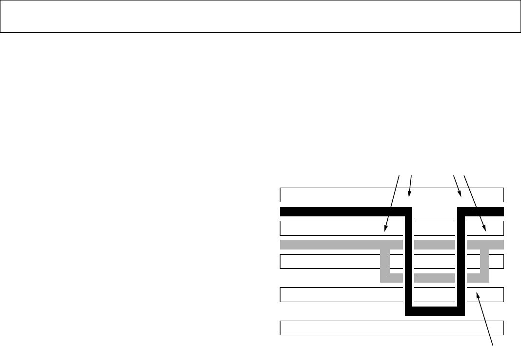
board stackup is shown in
Figure 22.
PCB DIELECTRIC
LAYER 1: SIGNAL (MICROSTRIP)
SILKSCREEN
SILKSCREEN
PCB DIELECTRIC
PCB DIELECTRIC
LAYER 2: GND (REFERENCE PLANE)
LAYER 3: PWR (REFERENCE PLANE)
LAYER 4: SIGNAL (MICROSTRIP)
W3W 3W
REFERENCE LAYER
RELIEVED UNDERNEATH
MICROSTRIP
07004-013
Figure 22. Example Board Stackup
HPD is a dc signal presented by a sink to a source to indicate
that the source EDID is available for reading. The placement
of this signal is not critical, but it should be routed as directly
as possible.
Power Supplies
The AD8194 has three separate power supplies referenced to
a single ground. The supply/ground pairs are
AVCC/AVEE
VTTI/AVEE
VTTO/AVEE
The AVCC/AVEE (3.3 V) supply powers the core of the
AD8194. The VTTI/AVEE supply (3.3 V) powers the input
termination (see
Figure 19). Similarly, the VTTO/AVEE
supply (3.3 V) powers the output termination (see
Figure 20).
In a typical application, all pins labeled AVEE should be con-
nected directly to ground. All pins labeled AVCC, VTTI, or
VTTO should be connected to 3.3 V. The supplies can also be
powered individually, but care must be taken to ensure that
each stage of the AD8194 is powered correctly.
Power Supply Bypassing
The AD8194 requires minimal supply bypassing. When
powering the supplies individually, place a 0.01 F capacitor
between each 3.3 V supply pin (AVCC, VTTI, and VTTO) and
ground to filter out supply noise. Generally, bypass capacitors
should be placed near the power pins and should connect directly
to the relevant supplies (without long intervening traces). For
example, to minimize the parasitic inductance of the power
supply decoupling capacitors, minimize the trace length between
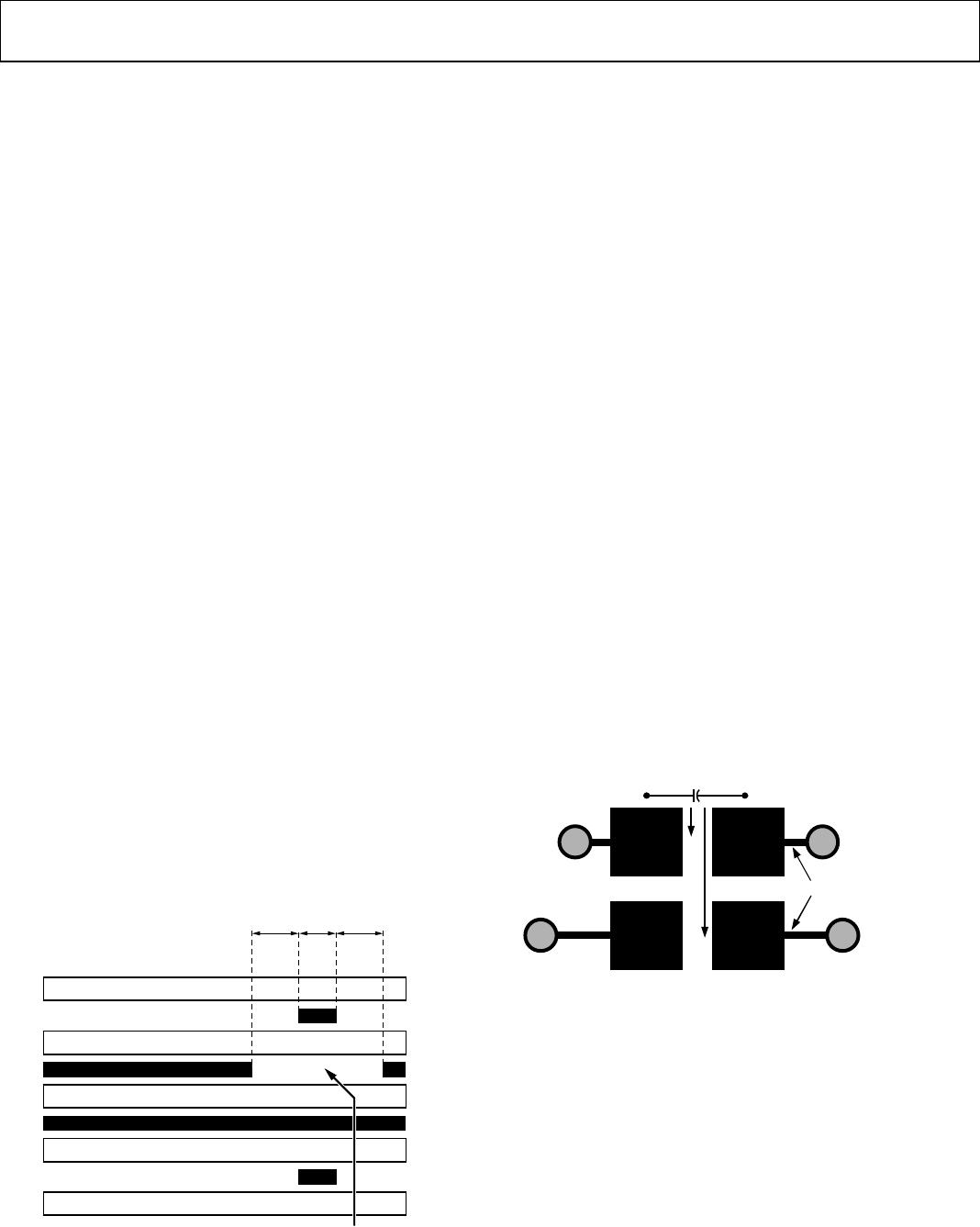
capacitor landing pads and the vias as shown in
Figure 23.
EXTRA ADDED INDUCTANCE
RECOMMENDED
NOT RECOMMENDED
07004-014
Figure 23. Recommended Pad Outline for Bypass Capacitors
In applications where the AD8194 is powered by a single 3.3 V
supply, it is recommended to use two reference supply planes
and bypass the 3.3 V reference plane to the ground reference
plane with one 220 pF, one 1000 pF, two 0.01 F, and one 4.7 F
capacitors. The capacitors should via down directly to the supply
planes and be placed within a few centimeters of the AD8194.
AD8194
Rev. 0 | Page 14 of 16
Evaluation Board
The AD8194 evaluation board illustrates one way to implement
a 2:1 HDMI link switch with an AD8194 and a CMOS switch.
The AD8194 evaluation board deviates from a typical
application in that it uses an HDMI connector for the output as
well as for the inputs. This setup makes it easy to connect
equipment to the AD8194 evaluation board with standard
HDMI cables. However, this arrangement requires crossing over
the TMDS signals on the output side (see
Figure 24).
In a typical application, the output of the AD8194 is routed
directly into an HDMI receiver. Because a receiver is generally
designed to interface directly to an HDMI input connector, it is
not necessary to cross over the TMDS signals in a typical
application (see
Figure 25).
CROSSOVER
REQUIRED
HDMI
CONNECTOR
1
19
19
AD8194
HDMI
CONNECTOR
1
1
19
HDMI
CONNECTOR
07004-027
Figure 24. Block Diagram of AD8194 Evaluation Board Showing Output Crossover
HDMI
CONNECTOR
HDMI
RECEIVER
1
19
AD8194
07004-026
Figure 25. HDMI Signals to HDMI Receiver, No Crossover Required

AD8194ACPZ

Mfr. #:
Manufacturer:
Analog Devices Inc.
Description:
Equalizers 2:1 TMDS Switch Buffered w/ Equal
Lifecycle:
New from this manufacturer.
Delivery:
DHL FedEx Ups TNT EMS
Payment:
T/T Paypal Visa MoneyGram Western Union

Products related to this Datasheet