3
FN8164.7
August 17, 2015
Pin Descriptions
Host Interface Pins
Serial Clock (SCL)
The SCL input is used to clock data into and out of the
X9241A.
Serial Data (SDA)
SDA is a bidirectional pin used to transfer data into and out
of the device. It is an open drain output and may be wire-
ORed with any number of open drain or open collector
outputs. An open drain output requires the use of a pull-up
resistor. For selecting typical values, refer to the guidelines
for calculating typical values on the bus pull-up resistors
graph.
Address
The Address inputs are used to set the least significant
4-bits of the 8-bit slave address. A match in the slave
address serial data stream must be made with the Address
input in order to initiate communication with the X9241A.
Potentiometer Pins
V
H
/R
H
(V
H0
/R
H0
TO V
H3
/R
H3
), V
L
/R
L
(V
L0
/R
L0
TO V
L3
/R
L3
)
The R
H
and R
L
inputs are equivalent to the terminal
connections on either end of a mechanical potentiometer.
V
W
/R
W
(V
W0
/R
W0
TO V
W3
/R
W3
)
The wiper outputs are equivalent to the wiper output of a
mechanical potentiometer.
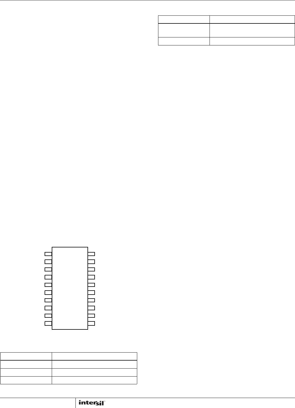
Pinout
X9241A
(20 LD DIP, SOIC, TSSOP)
TOP VIEW
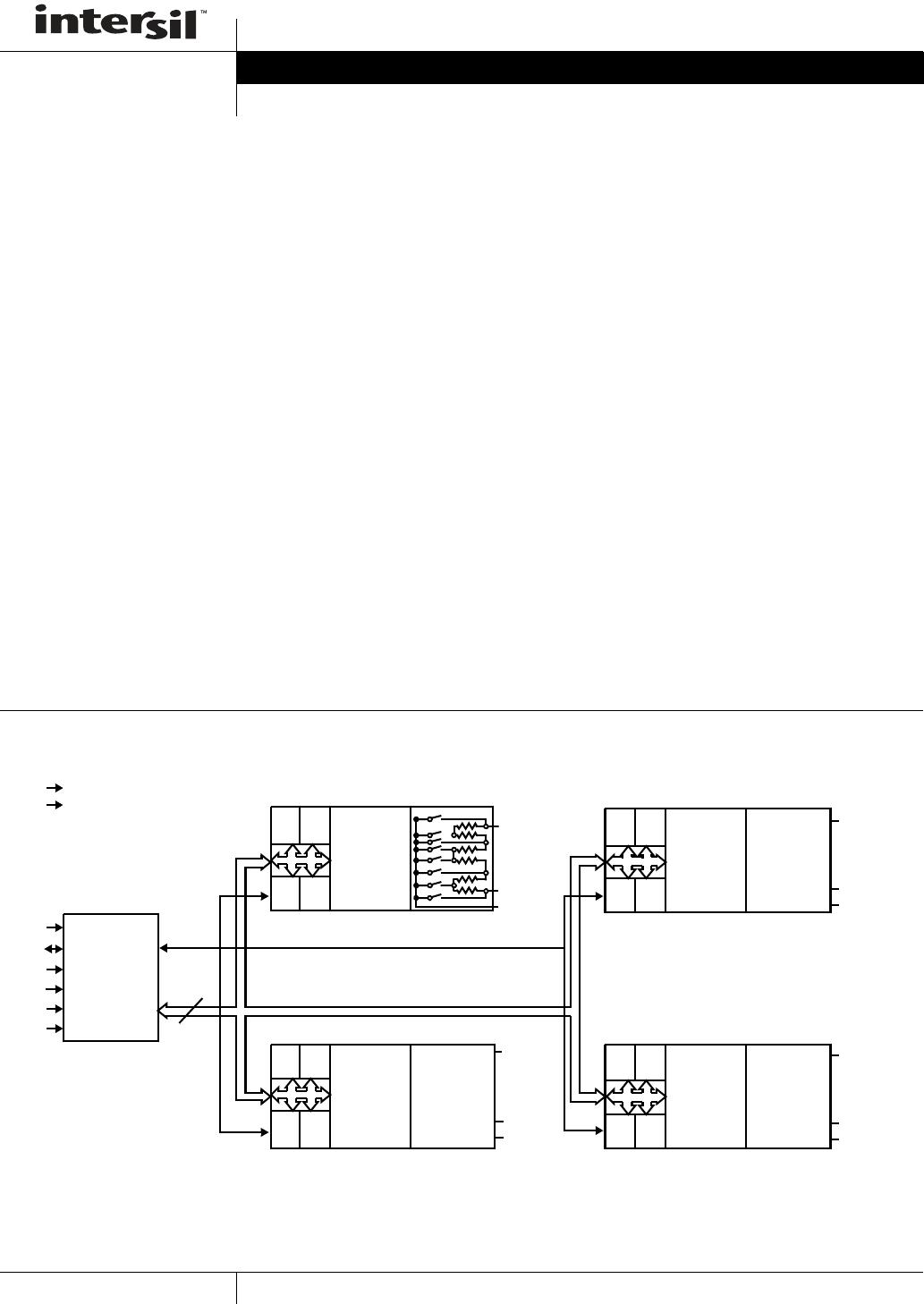
Principles of Operation
The X9241A is a highly integrated microcircuit incorporating
four resistor arrays, their associated registers and counters
and the serial interface logic providing direct communication
between the host and the XDCP potentiometers.
Serial Interface
The X9241A supports a bidirectional bus oriented protocol.
The protocol defines any device that sends data onto the
bus as a transmitter and the receiving device as the receiver.
The device controlling the transfer is a master and the
device being controlled is the slave. The master will always
initiate data transfers and provide the clock for both transmit
and receive operations. Therefore, the X9241A will be
considered a slave device in all applications.
Clock and Data Conventions
Data states on the SDA line can change only during SCL
LOW periods (t
LOW
). SDA state changes during SCL HIGH
are reserved for indicating start and stop conditions.
Start Condition
All commands to the X9241A are preceded by the start
condition, which is a HIGH to LOW transition of SDA while
SCL is HIGH (t
HIGH
). The X9241A continuously monitors the
SDA and SCL lines for the start condition and will not
respond to any command until this condition is met.
Stop Condition
All communications must be terminated by a stop condition,
which is a LOW to HIGH transition of SDA while SCL is
HIGH.
Acknowledge
Acknowledge is a software convention used to provide a
positive handshake between the master and slave devices
on the bus to indicate the successful receipt of data. The
transmitting device, either the master or the slave, will
release the SDA bus after transmitting 8-bits. The master
generates a ninth clock cycle and during this period the
receiver pulls the SDA line LOW to acknowledge that it
successfully received the 8-bits of data. See Figure 7.
The X9241A will respond with an acknowledge after
recognition of a start condition and its slave address and
once again after successful receipt of the command byte. If
the command is followed by a data byte the X9241A will
respond with a final acknowledge.
Pin Names
SYMBOL DESCRIPTION
SCL Serial Clock
SDA Serial Data
A0 to A3 Address
V
W0
/R
W0
A0
A2
V
H1
/R
H1
SDA
V
SS
1
2
3
4
5
6
7
8
9
10
20
19
18
17
16
15
14
13
12
11
V
CC
A1
A3
SCL
X9241A
V
L0
/R
L0
V
H0
/R
H0
V
W1
/R
W1
V
L1
/R
L1
V
W3
/R
W3
V
L3
/R
L3
V
H3
/R
H3
V
W2
/R
W2
V
L2
/R
L2
V
H2
/R
H2
V
H0
/R
H0
to V
H3
/R
H3
,
V
L0
/R
L0
to V
L3
/R
L3
Potentiometer Pins (terminal equivalent)
V
W0
/R
W0
to V
W3
/R
W3
Potentiometer Pins (wiper equivalent)
Pin Names
SYMBOL DESCRIPTION
X9241A