10
FN8164.7
August 17, 2015
Absolute Maximum Ratings Thermal Information
Supply Voltage (V
CC
) Limits
X9241A. . . . . . . . . . . . . . . . . . . . . . . . . . . . . . . . . . . . . . 5V ±10%
Max Wiper Current for 2k R
TOTAL
. . . . . . . . . . . . . . . . . . . . . . ±4mA
Max Wiper Current for 10k and 50k R
TOTAL
. . . . . . . . . . . . . . ±3mA
Voltage on SCK, SCL or any address
input with respect to V
SS
. . . . . . . . . . . . . . . . . . . . . . . -1V to +7V
Voltage on any V
H
/R
H
, V
W
/R
W
or V
L
/R
L
referenced to V
SS
. . . . . . . . . . . . . . . . . . . . . . . . . . . . . . +6V/-4V
V = |V
H
/R
H
- V
L
/R
L
|. . . . . . . . . . . . . . . . . . . . . . . . . . . . . . . . . .10V
I
W
(10s) . . . . . . . . . . . . . . . . . . . . . . . . . . . . . . . . . . . . . . . . . . ±6mA
Power rating (each pot) . . . . . . . . . . . . . . . . . . . . . . . . . . . . . .50mW
Temperature under bias. . . . . . . . . . . . . . . . . . . . . . . . -65 to +135°C
Storage temperature . . . . . . . . . . . . . . . . . . . . . . . . . . -65 to +150°C
Pb-free reflow profile . . . . . . . . . . . . . . . . . . . . . . . . . .see link below
http://www.intersil.com/pbfree/Pb-FreeReflow.asp
Recommended Operating Conditions
Temperature (Commercial) . . . . . . . . . . . . . . . . . . . . . 0°C to +70°C
Temperature (Industrial). . . . . . . . . . . . . . . . . . . . . . . -40°C to +85°C
CAUTION: Do not operate at or near the maximum ratings listed for extended periods of time. Exposure to such conditions may adversely impact product reliability and
result in failures not covered by warranty.
Analog Specifications (Over recommended operating conditions unless otherwise stated).
SYMBOL PARAMETER TEST CONDITION
LIMITS
UNIT
MIN
(Note 11) TYP
MAX
(Note 11)
R
TOTAL
End to end resistance -20 +20 %
R
W
Wiper resistance Wiper Current = (V
H
- V
L
)/R
TOTAL
40 130
V
TERM
Voltage on any V
H
/R
H
, V
W
/R
W
or V
L
/R
L
Pin -3.0 +5 V
Noise Ref: 1kHz (Note 7) 120 dBV
Resolution (Note 7) 1.6 %
Absolute linearity (Note 3) R
w(n)(actual)
- R
w(n)(expected)
±1 MI (Note 5)
Relative linearity
(Note 4) R
w(n + 1)
- [R
w(n) + MI
] ±0.2 MI (Note 5)
Temperature coefficient of R
TOTAL
(Note 7) ±300 ppm/°C
Ratiometric temperature coefficient (Note 7) ±20 ppm/C
C
H
/C
L
/C
W
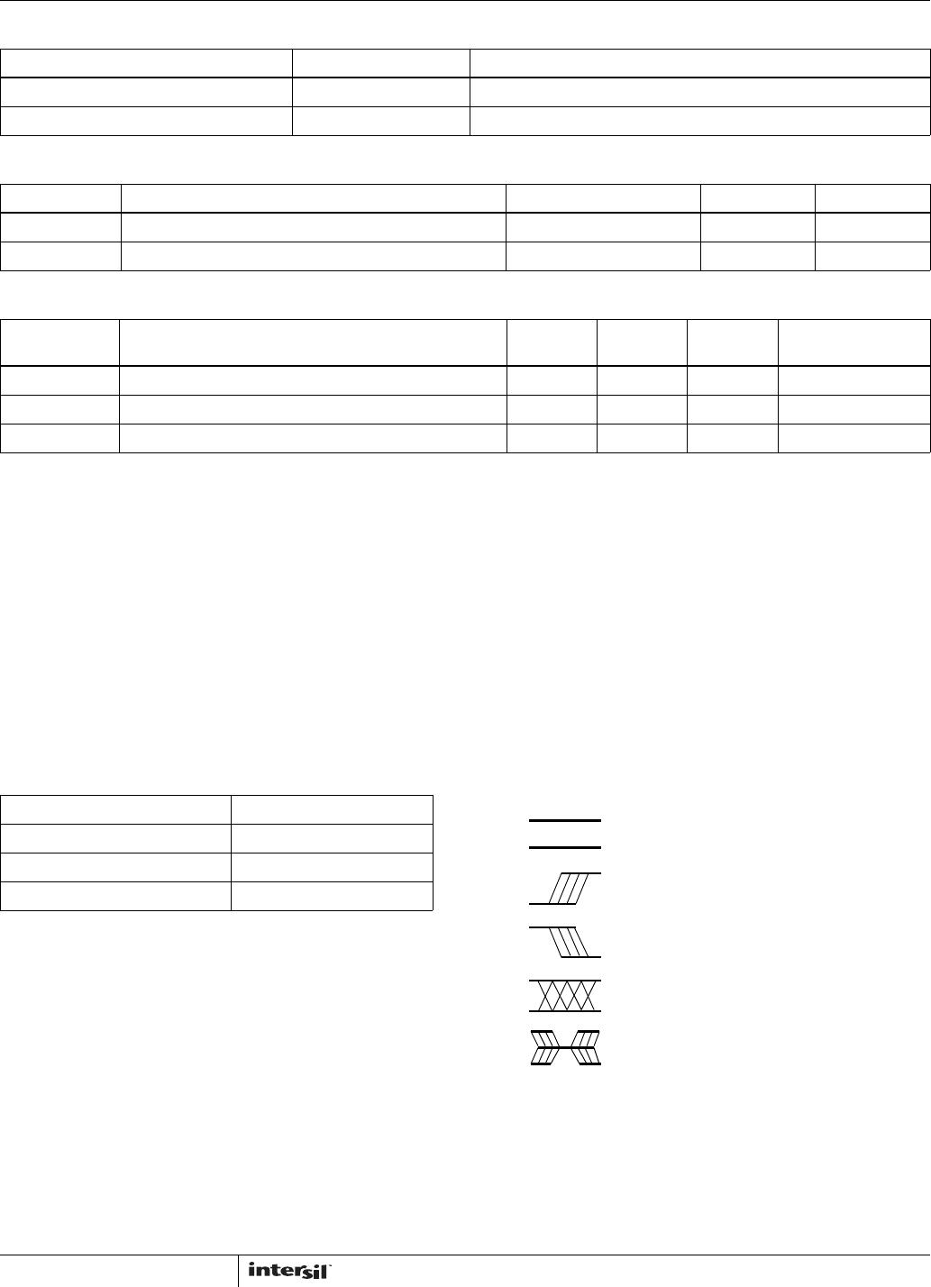
Potentiometer capacitances See Circuit #3 and (Note 7) 15/15/25 pF
l
AL
R
H
, R
I
, R
W
leakage current V
IN
= V
TERM
. Device is in stand-by mode. 0.1 1 µA
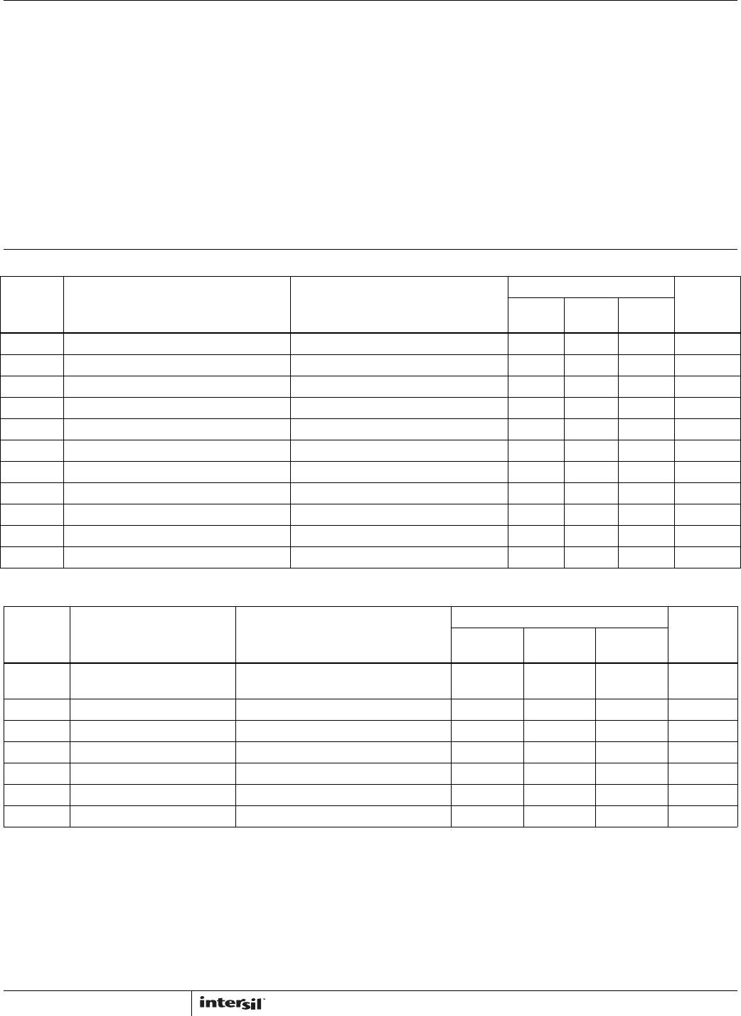
DC Electrical Specifications (Over recommended operating conditions unless otherwise stated.)
SYMBOL PARAMETER TEST CONDITION
LIMITS
UNIT
MIN
(Note 11) TYP
MAX
(Note 11)
l
CC
Supply current (active) f
SCL
= 100kHz, Write/Read to WCR,
Other Inputs = V
SS
3mA
I
SB
V
CC
current (standby) SCL = SDA = V
CC
, Addr. = V
SS
200 500 µA
I
LI
Input leakage current V
IN
= V
SS
to V
CC
10 µA
I
LO
Output leakage current V
OUT
= V
SS
to V
CC
10 µA
V
IH
Input HIGH voltage 2 V
V
IL
Input LOW voltage 0.8 V
V
OL
Output LOW voltage I
OL
= 3mA 0.4 V
NOTES:
3. Absolute Linearity is utilized to determine actual wiper voltage versus expected voltage as determined by wiper position when used as a
potentiometer.
4. Relative Linearity is utilized to determine the actual change in voltage between two successive tap positions when used as a potentiometer. It is
a measure of the error in step size.
5. MI = RTOT/63 or (R
H
– R
L
)/63, single pot
6. Max = all four arrays cascaded together, Typical = individual array resolutions.
X9241A
11
FN8164.7
August 17, 2015
Power-up Requirements (Power Up sequencing can affect correct recall of the wiper registers)
The preferred power-on sequence is as follows: First V
CC
, then the potentiometer pins. It is suggested that Vcc reach 90% of its
final value before power is applied to the potentiometer pins. The V
CC
ramp rate specification should be met, and any glitches or
slope changes in the V
CC
line should be held to <100mV if possible. Also, V
CC
should not reverse polarity by more than 0.5V.
NOTES:
7. Limits should be considered typical and are not production tested.
8. Limits established by characterization and are not production tested.
9. Maximum Wiper Current is derated over temperature. See the Wiper Current Derating Curve.
10. T
i
value denotes the maximum noise glitch pulse width that the device will ignore on either SCL or SDA pins. Any noise glitch pulse width that
is greater than this maximum value will be considered as a valid clock or data pulse and may cause communication failure to the device.
11. Parts are 100% tested at either +70°C or +85°C. Over temperature limits established by characterization and are not production tested.
Symbol Table
Endurance and Data Retention
PARAMETER MIN UNIT
Minimum endurance 100,000 Data changes per bit per register
Data retention 100 Years
Capacitance
SYMBOL PARAMETER TEST CONDITION TYP UNIT
C
I/O
(Note 7) Input/output capacitance (SDA) V
I/O
= 0V 19 pF
C
IN
(Note 7) Input capacitance (A0, A1, A2, A3 and SCL) V
IN
= 0V 12 pF
Power-up Timing
SYMBOL PARAMETER
MIN
(Note 11) TYP
MAX
(Note 11) UNIT
t
PUR
(Note 8) Power-up to initiation of read operation 1 ms
t
PUW
(Note 8) Power-up to initiation of write operation 5 ms
t
R
V
CC
V
CC
Power up ramp rate 0.2 50 V/ms
AC Conditions of Test
Input pulse levels V
CC
x 0.1 to V
CC
x 0.9
Input rise and fall times 10ns
Input and output timing levels V
CC
x 0.5
Input pulse levels V
CC
x 0.1 to V
CC
x 0.9
WAVEFORM INPUTS OUTPUTS
Must be
steady
Will be
steady
May change
from LOW
to HIGH
Will change
from LOW
to HIGH
May change
from HIGH
to LOW
Will change
from HIGH
to LOW
Dont Care:
Changes
Allowed
Changing:
State Not
Known
N/A Center Line
is High
Impedance
X9241A
12
FN8164.7
August 17, 2015
Equivalent AC Test Circuit
Circuit #3 SPICE Macro Model
Guidelines for Calculating
Typical Values of Bus Pull-Up Resistors
DCP Wiper Current De-rating Curve
5V
1533
100pF
SDA OUTPUT
R
H
C
H
15pF
C
W
R
L
C
L
R
W
R
TOTAL
25pF
15pF
MACRO MODEL
7
6
5
3
4
1
20 40 60 70 80 90
0
0
AMBIENT TEMPERATURE (°C)
MAXIMUM DCP WIPER CURRENT
2
5010 30
AC Electrical Specifications (Over recommended operating conditions unless otherwise stated).
SYMBOL PARAMETER
LIMITS
UNIT
REFERENCE
FIGURE
NUMBER(S)
MIN
(Note 11)
MAX
(Note 11)
f
SCL
SCL clock frequency 0 100 kHz 10
t
LOW
Clock LOW period 4700 ns 10
t
HIGH
Clock HIGH period 4000 ns 10
t
R
SCL and SDA rise time 1000 ns 10
t
F
SCL and SDA fall time 300 ns 10
T
i
,
(Note 11) Noise suppression time constant (glitch filter) 20 ns 10
t
SU:STA
Start condition setup time (for a repeated start condition) 4000 ns 10 and 12
t
HD:STA
Start condition hold time 4000 ns 10 and 12
t
HIGH
t
SU:STA
t
HD:STA
t
HD:DAT
t
SU:DAT
t
LOW
t
F
t
SU:STO
t
R
t
BUF
SCL
SDA
(DATA IN)
FIGURE 10. INPUT BUS TIMING
X9241A

X9241AUVIZT1

Mfr. #:
Manufacturer:
Renesas / Intersil
Description:
Digital Potentiometer ICs QD CMOS EEPOT 50KOHM S
Lifecycle:
New from this manufacturer.
Delivery:
DHL FedEx Ups TNT EMS
Payment:
T/T Paypal Visa MoneyGram Western Union