13
FN8164.7
August 17, 2015
t
SU:DAT
Data in setup time 250 ns 10
t
HD:DAT
Data in hold time 0 ns 10
t
AA
SCL LOW to SDA data out valid 3500 ns 11
t
DH
Data out hold time 30 ns 11
t
SU:STO
Stop condition setup time 4000 ns 10 and 12
t
BUF
Bus free time prior to new transmission 4700 ns 10
t
WR
Write cycle time (nonvolatile write operation) 10 ms 13
t
STPWV
Wiper response time from stop generation 500 µs 13
t
CLWV
Wiper response from SCL LOW 1000 µs 6
AC Electrical Specifications (Over recommended operating conditions unless otherwise stated). (Continued)
SYMBOL PARAMETER
LIMITS
UNIT
REFERENCE
FIGURE
NUMBER(S)
MIN
(Note 11)
MAX
(Note 11)
t
AA
t
DH
SCL
SDA
SDA
OUT
(ACK) SDA
OUT
SDA
OUT
FIGURE 11. OUTPUT BUS TIMING
t
SU:STO
SCL
SDA
t
HD:STA
t
SU:STA
STOP CONDITIONSTART CONDITION
(DATA IN)
FIGURE 12. START STOP TIMING
SCL
SDA
WIPER
OUTPUT
CLOCK 8
SDA
IN
CLOCK 9
ACK
STOP
t
WR
t
STPWV
START
FIGURE 13. WRITE CYCLE AND WIPER RESPONSE TIMING
X9241A
14
FN8164.7
August 17, 2015
About Intersil
Intersil Corporation is a leading provider of innovative power management and precision analog solutions. The company's products
address some of the largest markets within the industrial and infrastructure, mobile computing and high-end consumer markets.
For the most updated datasheet, application notes, related documentation and related parts, please see the respective product
information page found at www.intersil.com.
You may report errors or suggestions for improving this datasheet by visiting www.intersil.com/ask
.
Reliability reports are also available from our website at
www.intersil.com/support
Revision History
The revision history provided is for informational purposes only and is believed to be accurate, but not warranted. Please go to the web to make
sure that you have the latest revision.
DATE REVISION CHANGE
August 17, 2015 FN8164.7 - Ordering Information Table on page 2.
- Added Revision History beginning with Rev 1.
- Added About Intersil Verbiage.
X9241A
15
FN8164.7
August 17, 2015
X9241A
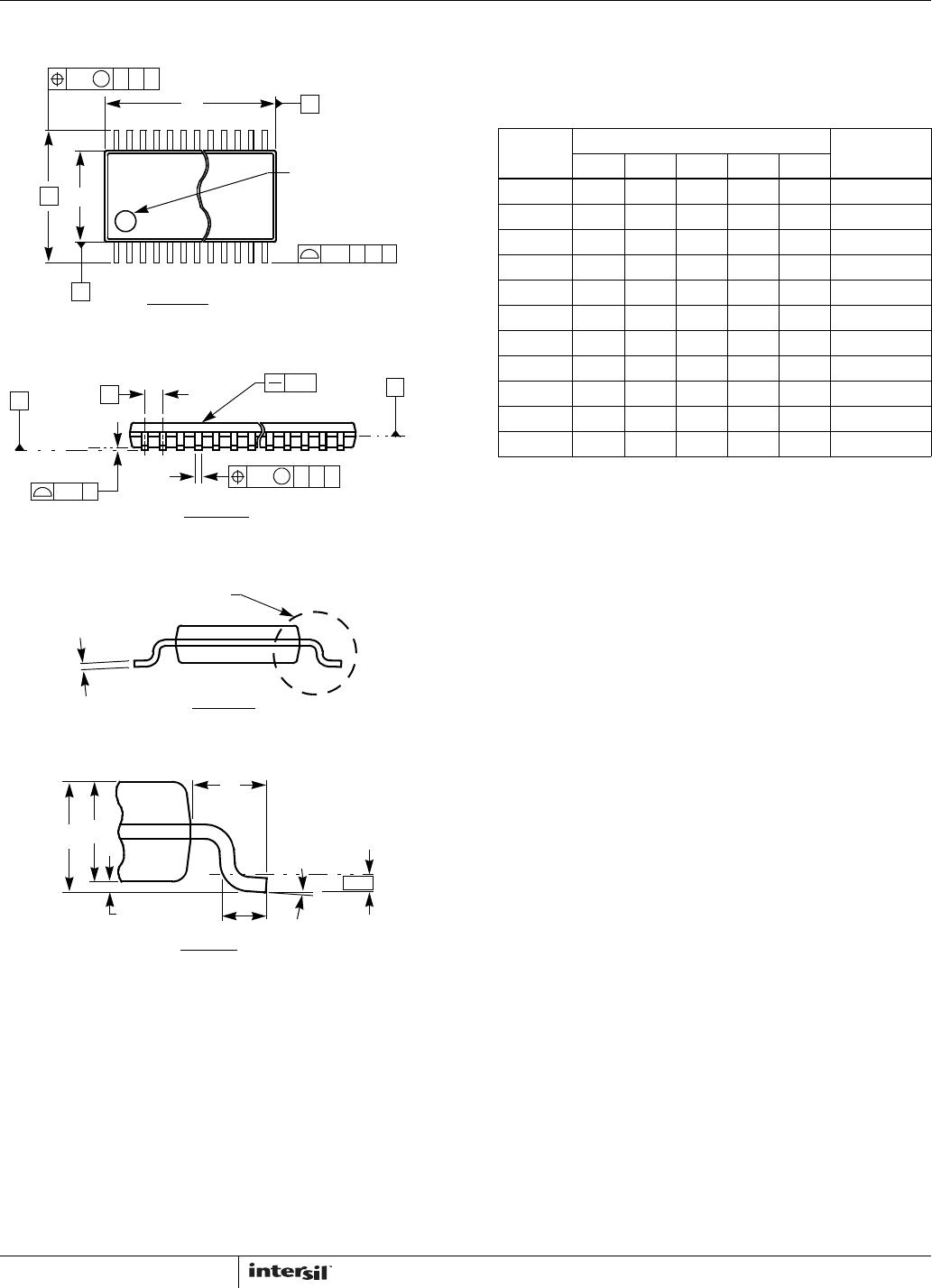
Thin Shrink Small Outline Package Family (TSSOP)
N
(N/2)+1
(N/2)
TOP VIEW
AD
0.20 C
2X
B A
N/2 LEAD TIPS
B
E1
E
0.25 CAB
M
1
H
PIN #1 I.D.
0.05
e
C
0.10 C
N LEADS
SIDE VIEW
0.10 CABM
b
c
SEE DETAIL “X”
END VIEW
DETAIL X
A2
0° - 8°
GAUGE
PLANE
0.25
L
A1
A
L1
SEATING
PLANE
MDP0044
THIN SHRINK SMALL OUTLINE PACKAGE FAMILY
SYMBOL
MILLIMETERS
TOLERANCE14 LD 16 LD 20 LD 24 LD 28 LD
A 1.20 1.20 1.20 1.20 1.20 Max
A1 0.10 0.10 0.10 0.10 0.10 ±0.05
A2 0.90 0.90 0.90 0.90 0.90 ±0.05
b 0.25 0.25 0.25 0.25 0.25 +0.05/-0.06
c 0.15 0.15 0.15 0.15 0.15 +0.05/-0.06
D 5.00 5.00 6.50 7.80 9.70 ±0.10
E 6.40 6.40 6.40 6.40 6.40 Basic
E1 4.40 4.40 4.40 4.40 4.40 ±0.10
e 0.65 0.65 0.65 0.65 0.65 Basic
L 0.60 0.60 0.60 0.60 0.60 ±0.15
L1 1.00 1.00 1.00 1.00 1.00 Reference
Rev. F 2/07
NOTES:
1. Dimension “D” does not include mold flash, protrusions or gate
burrs. Mold flash, protrusions or gate burrs shall not exceed
0.15mm per side.
2. Dimension “E1” does not include interlead flash or protrusions.
Interlead flash and protrusions shall not exceed 0.25mm per
side.
3. Dimensions “D” and “E1” are measured at dAtum Plane H.
4. Dimensioning and tolerancing per ASME Y14.5M-1994.

X9241AUVIZT1

Mfr. #:
Manufacturer:
Renesas / Intersil
Description:
Digital Potentiometer ICs QD CMOS EEPOT 50KOHM S
Lifecycle:
New from this manufacturer.
Delivery:
DHL FedEx Ups TNT EMS
Payment:
T/T Paypal Visa MoneyGram Western Union