4
FN8164.7
August 17, 2015
Array Description
The X9241A is comprised of four resistor arrays. Each array
contains 63 discrete resistive segments that are connected
in series. The physical ends of each array are equivalent to
the fixed terminals of a mechanical potentiometer (V
H
/R
H
and V
L
/R
L
inputs).
At both ends of each array and between each resistor
segment is a FET switch connected to the wiper (V
W
/R
W
)
output. Within each individual array only one switch may be
turned on at a time. These switches are controlled by the
Wiper Counter Register (WCR). The 6 least significant bits of
the WCR are decoded to select, and enable, 1 of 64
switches.
The WCR may be written directly, or it can be changed by
transferring the contents of one of four associated Data
Registers into the WCR. These Data Registers and the WCR
can be read and written by the host system.
Device Addressing
Following a start condition the master must output the
address of the slave it is accessing. The most significant
4-bits of the slave address are the device type identifier
(refer to Figure 1). For the X9241A, this is fixed as 0101[B].
The next 4-bits of the slave address are the device address.
The physical device address is defined by the state of the A0
to A3 inputs. The X9241A compares the serial data stream
with the address input state; a successful compare of all 4
address bits is required for the X9241A to respond with an
acknowledge.
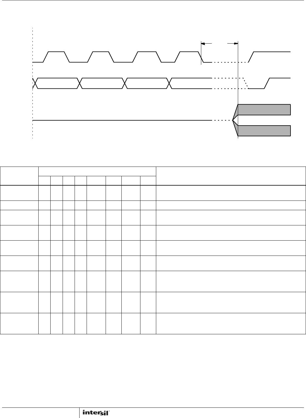
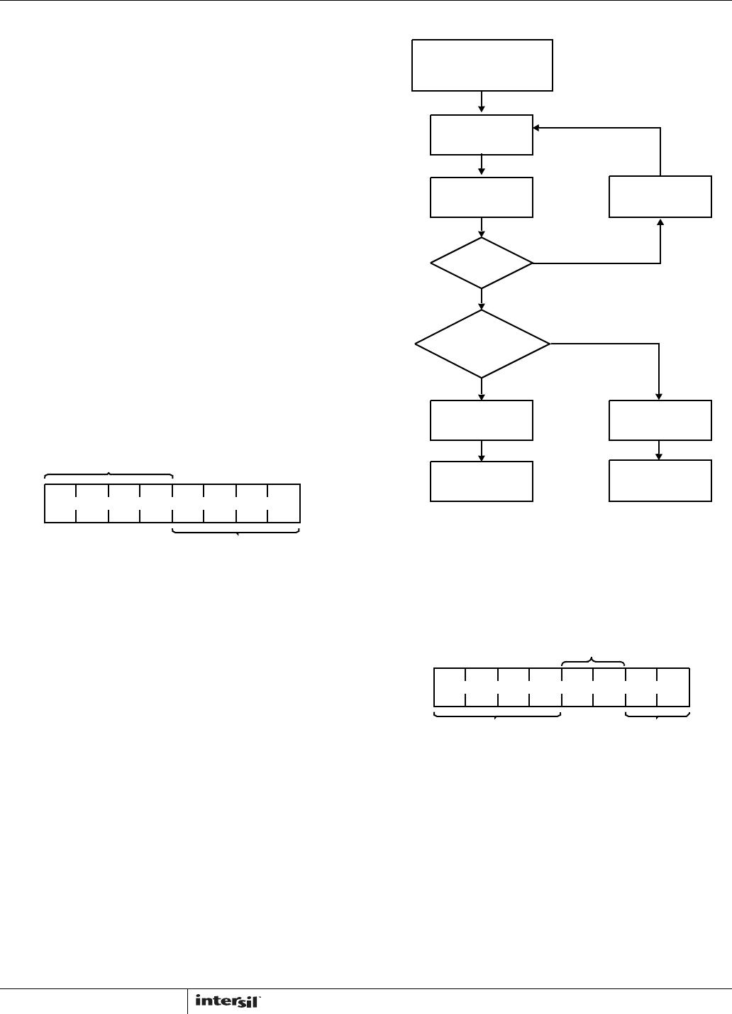
Acknowledge Polling
The disabling of the inputs, during the internal nonvolatile
write operation, can be used to take advantage of the typical
5ms EEPROM write cycle time. Once the stop condition is
issued to indicate the end of the nonvolatile write command,
the X9241A initiates the internal write cycle. ACK polling can
be initiated immediately. This involves issuing the start
condition followed by the device slave address. If the
X9241A is still busy with the write operation, no ACK will be
returned. If the X9241A has completed the write operation,
an ACK will be returned and the master can then proceed
with the next operation.
Flow 1. ACK Polling Sequence
Instruction Structure
The next byte sent to the X9241A contains the instruction
and register pointer information. The 4 most significant bits
are the instruction. The next 4-bits point to one of four pots
and when applicable they point to one of four associated
registers. The format is in Figure 2.
The 4 high order bits define the instruction. The next 2-bits
(P1 and P0) select which one of the four potentiometers is to
be affected by the instruction. The last 2-bits (R1 and R0)
select one of the four registers that are to be acted upon
when a register oriented instruction is issued.
Four of the nine instructions end with the transmission of the
instruction byte. The basic sequence is illustrated in Figure 3.
These two-byte instructions exchange data between the WCR
and one of the data registers. A transfer from a Data Register
to a WCR is essentially a write to a static RAM. The response
10 0 A3 A2 A1 A0
DEVICE TYPE
IDENTIFIER
DEVICE ADDRESS
1
FIGURE 1. SLAVE ADDRESS
NONVOLATILE WRITE
COMMAND COMPLETED
ENTER ACK POLLING
ISSUE
START
ISSUE SLAVE
ADDRESS
ACK
RETURNED?
FURTHER
OPERATION?
ISSUE
INSTRUCTION
PROCEED
ISSUE STOP
NO
YES
YES
PROCEED
ISSUE STOP
NO
I1I2I3 I0 P1 P0 R1 R0
POTENTIOMETER
SELECT
REGISTER
SELECT
INSTRUCTIONS
FIGURE 2. INSTRUCTION BYTE FORMAT
X9241A