X28HC64
10
FN8109.4
June 27, 2016
Submit Document Feedback
Power-Up Timing
PARAMETER SYMBOL
TYP
(Note 11)UNIT
Power-Up to Read Operation (Note 13
)t
PUR
100 µs
Power-Up to Write Operation (Note 13
)t
PUW
5ms
Capacitance T
A
= +25°C, f = 1MHz, V
CC
= 5V
PARAMETER SYMBOL TEST CONDITIONS MAX UNIT
Input/output Capacitance (Note 13
)C
I/O
V
I/O
= 0V 10 pF
Input Capacitance (Note 13
)C
IN
V
IN
= 0V 6 pF
NOTE:
13. This parameter is periodically sampled and not 100% tested.
TABLE 1. AC CONDITIONS OF TEST
Input Pulse Levels 0V to 3V
Input Rise and Fall Times 5ns
Input and Output Timing Levels 1.5V
TABLE 2. MODE SELECTION
CE
OE WE MODE I/O POWER
LLHRead D
OUT
Active
LHLWrite D
IN
Active
HXXStandby and write
inhibit
High Z Standby
XLXWrite inhibit
-
-
XXHWrite inhibit - -
Equivalent AC Load Circuits
FIGURE 13. EQUIVALENT AC LOAD CIRCUITS
5V
1.92kΩ
30pF
OUTPUT
1.37kΩ
Symbol Table
WAVEFORM INPUTS OUTPUTS
Must be
steady
Will be
steady
Ma y change
from LOW
to HIGH
Will change
from LOW
to HIGH
Ma y change
from HIGH
to LOW
Will change
from HIGH
to LOW
Don’t Care:
Changes
Allowed
Changing:
State Not
Known
N/A Center Line
is High
Impedance
X28HC64
11
FN8109.4
June 27, 2016
Submit Document Feedback
AC Electrical Specifications
Read Cycle Limits Over the recommended operating conditions unless otherwise specified.
PARAMETER SYMBOL
X28HC64-70 X28HC64-90 X28HC64-12
UNIT
MIN
(Note 10
)
MAX
(Note 10)
MIN
(Note 10)
MAX
(Note 10)
MIN
(Note 10)
MAX
(Note 10)
Read Cycle Time t
RC
70 90 120 ns
Chip Enable Access Time t
CE
70 90 120 ns
Address Access Time t
AA
70 90 120 ns
Output Enable Access Time t
OE
35 40 50 ns
CE LOW to Active Output (Note 14)t
LZ
000 ns
OE
LOW to Active Output (Note 14)t
OLZ
000 ns
CE
HIGH to High Z Output (Note 14)t
HZ
30 30 30 ns
OE HIGH to High Z Output (Note 14)t
OHZ
30 30 30 ns
Output Hold from Address Change t
OH
000ns
NOTE:
14. t
LZ
minimum, t
HZ
, t
OLZ
minimum, and t
OHZ
are periodically sampled and not 100% tested. t
HZ
maximum and t
OHZ
maximum are measured from the
point when CE
or OE return HIGH (whichever occurs first) to the time when the outputs are no longer driven.
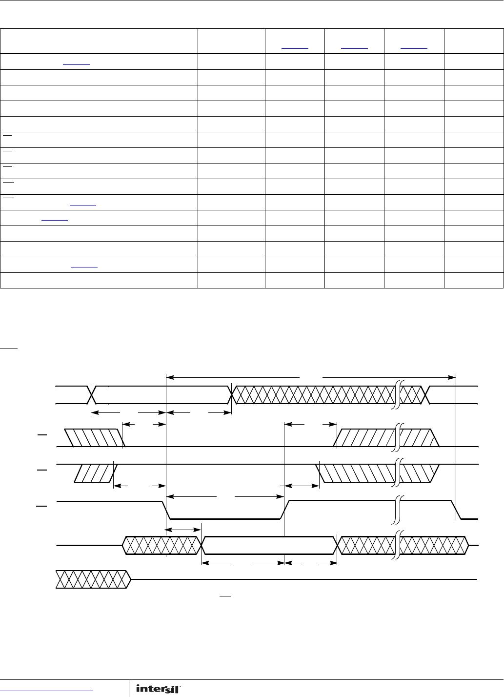
Read Cycle
FIGURE 14. READ CYCLE
t
CE
t
RC
ADDRESS
CE
OE
WE
DATA VALID
t
OE
t
LZ
t
OLZ
t
OH
t
AA
t
HZ
t
OHZ
DATA I/O
V
IH
HIGH Z
DATA VALID
X28HC64
12
FN8109.4
June 27, 2016
Submit Document Feedback
Write Cycle Limits
PARAMETER SYMBOL
MIN
(Note 10)
TYP
(Note 11)
MAX
(Note 10)UNIT
Write Cycle Time (Note 15
)t
WC
25ms
Address Set-Up Time t
AS
0ns
Address Hold Time t
AH
50 ns
Write Set-Up Time t
CS
0ns
Write Hold Time t
CH
0ns
CE
Pulse Width t
CW
50 ns
OE
High Set-Up Time t
OES
0ns
OE High Hold Time t
OEH
0ns
WE
Pulse Width t
WP
50 ns
WE
HIGH Recovery (Note 16)t
WPH
50 ns
Data Valid (Note 16)t
DV
s
Data Setup t
DS
50 ns
Data Hold t
DH
0ns
Delay to Next Write (Note 16)t
DW
10 µs
Byte Load Cycle t
BLC
0.15 100 µs
NOTES:
15. t
WC
is the minimum cycle time to be allowed from the system perspective unless polling techniques are used. It is the maximum time the device
requires to automatically complete the internal write operation.
16. t
WPH
and t
DW
are periodically sampled and not 100% tested.
WE Controlled Write Cycle
FIGURE 15. WE CONTROLLED WRITE CYCLE
ADDRESS
t
AS
t
WC
t
AH
t
OES
t
DS
t
DH
t
OEH
CE
WE
OE
DATA IN
DATA OUT
HIGH Z
t
CS
t
CH
t
WP
t
DV
DATA VALID

X28HC64JIZ-90

Mfr. #:
Manufacturer:
Renesas / Intersil
Description:
EEPROM 8K X 8 EEPROM CMOS 3
Lifecycle:
New from this manufacturer.
Delivery:
DHL FedEx Ups TNT EMS
Payment:
T/T Paypal Visa MoneyGram Western Union

Products related to this Datasheet