2.5 V/3.0 V
High Precision Reference
Data Sheet
AD780
Rev. H Document Feedback
Information furnished by Analog Devices is believed to be accurate and reliable. However, no
responsibility is assumed by Analog Devices for its use, nor for any infringements of patents or other
rights of third parties that may result from its use. Specifications subject to change without notice. No
license is granted by implication or otherwise under any patent or patent rights of Analog Devices.
Trademarks and registered trademarks are the property of their respective owners.
One Technology Way, P.O. Box 9106, Norwood, MA 02062-9106, U.S.A.
Tel: 781.329.4700 ©19932015 Analog Devices, Inc. All rights reserved.
Technical Support www.analog.com
FEATURES
Pin programmable 2.5 V or 3.0 V output
Ultralow drift: 3 ppm/°C max
High accuracy: 2.5 V or 3.0 V ±1 mV max
Low noise: 100 nV/√
Hz
Noise reduction capability
Low quiescent current: 1 mA max
Output trim capability
Plug-in upgrade for present references
Temperature output pin
Series or shunt mode operation (±2.5 V, ±3.0 V)
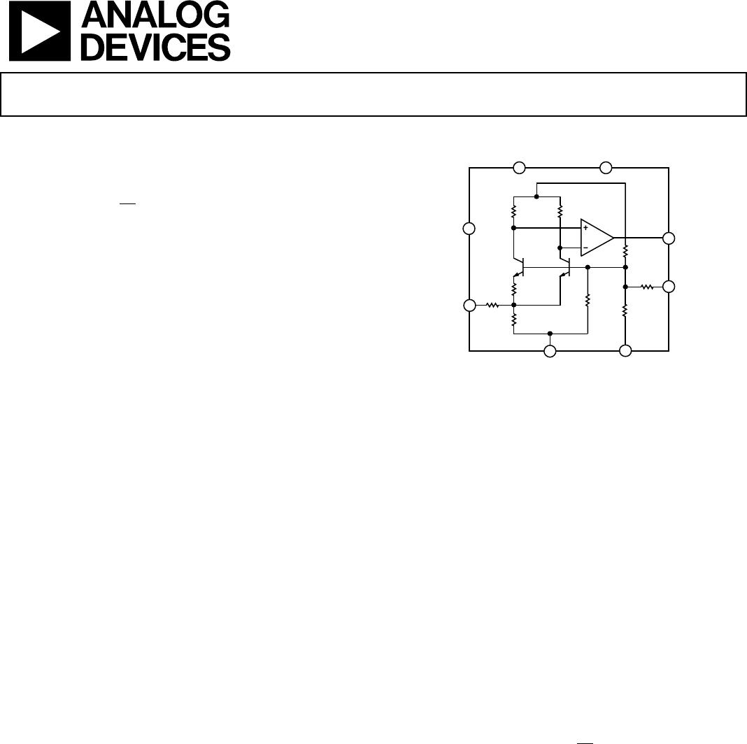
FUNCTIONAL BLOCK DIAGRAM
00841-001
R16
R10
+V
IN
R4
R5
Q6
Q7
R11
R14
R13
R15
DNC
V
OUT
TRIM
GND
O/P SELECT
2.5V – DNC
3.0V – GND
TEMP
DNC
DNC = DO NOT CONNECT TO THIS PIN
AD780
72
1
3
4 8
5
6
Figure 1.
GENERAL DESCRIPTION
The AD780 is an ultrahigh precision band gap reference voltage
that provides a 2.5 V or 3.0 V output from inputs between 4.0 V
and 36 V. Low initial error and temperature drift combined with
low output noise and the ability to drive any value of capacitance
make the AD780 the ideal choice for enhancing the performance
of high resolution analog-to-digital converters (ADCs) and
digital-to-analog converters (DACs), and for any general-purpose
precision reference application. A unique low headroom design
facilitates a 3.0 V output from a 5.0 V 10% input, providing a
20% boost to the dynamic range of an ADC over performance
with existing 2.5 V references.
The AD780 can be used to source or sink up to 10 mA, and can
be used in series or shunt mode, thus allowing positive or negative
output voltages without external components. This makes it
suitable for virtually any high performance reference application.
Unlike some competing references, the AD780 has no region of
possible instability. The part is stable under all load conditions
when a 1 µF bypass capacitor is used on the supply.
A temperature output pin on the AD780 provides an output
voltage that varies linearly with temperature, allowing the part
to be configured as a temperature transducer while providing a
stable 2.5 V or 3.0 V output.
The AD780 is a pin compatible performance upgrade for the
LT1019(A)2.5 and the AD680. The latter is targeted toward
low power applications.
The AD780 is available in three grades in PDIP and SOIC
packages. The AD780AN, AD780AR, AD780BN, AD780BR,
and AD780CR are specified for operation from −40°C to +85°C.
PRODUCT HIGHLIGHTS
1. The AD780 provides a pin programmable 2.5 V or 3.0 V
output from a 4 V to 36 V input.
2. Laser trimming of both initial accuracy and temperature
coefficients results in low errors over temperature without
the use of external components. The AD780BN has a
maximum variation of 0.9 mV from −40°C to +85°C.
3. For applications that require even higher accuracy, an
optional fine-trim connection is provided.
4. The AD780 noise is extremely low, typically 4 mV p-p
from 0.1 Hz to 10 Hz and a wideband spectral noise
density of typically 100 nV/√
Hz
. This can be further
reduced, if desired, by using two external capacitors.
5. The temperature output pin enables the AD780 to be
configured as a temperature transducer while providing a
stable output reference.
AD780* PRODUCT PAGE QUICK LINKS
Last Content Update: 02/23/2017
COMPARABLE PARTS
View a parametric search of comparable parts.
DOCUMENTATION
Application Notes
AN-713: The Effect of Long-Term Drift on Voltage
References
Data Sheet
AD780: 2.5 V/3.0 V High Precision Reference Data Sheet
AD780: Military Data Sheet
TOOLS AND SIMULATIONS
AD780 SPICE Macro-Model
REFERENCE DESIGNS
CN0030
CN0044
CN0047
CN0100
CN0116
DESIGN RESOURCES
AD780 Material Declaration
PCN-PDN Information
Quality And Reliability
Symbols and Footprints
DISCUSSIONS
View all AD780 EngineerZone Discussions.
SAMPLE AND BUY
Visit the product page to see pricing options.
TECHNICAL SUPPORT
Submit a technical question or find your regional support
number.
DOCUMENT FEEDBACK
Submit feedback for this data sheet.
This page is dynamically generated by Analog Devices, Inc., and inserted into this data sheet. A dynamic change to the content on this page will not
trigger a change to either the revision number or the content of the product data sheet. This dynamic page may be frequently modified.
AD780 Data Sheet
Rev. H | Page 2 of 12
TABLE OF CONTENTS
Features .............................................................................................. 1
Functional Block Diagram .............................................................. 1
General Description ......................................................................... 1
Product Highlights ........................................................................... 1
Revision History ............................................................................... 2
Specifications ..................................................................................... 3
Absolute Maximum Ratings ............................................................ 4
Notes ............................................................................................... 4
ESD Caution .................................................................................. 4
Theory of Operation ........................................................................ 5
Applying the AD780 ......................................................................... 6
Noise Performance ....................................................................... 6
Noise Comparison ........................................................................ 7
Temperature Performance ........................................................... 7
Temperature Output Pin ..............................................................7
Temperature Transducer Circuit .................................................8
Supply Current Over Temperature .............................................8
Turn-On Time ...............................................................................8
Dynamic Performance ..................................................................9
Line Regulation ..............................................................................9
Precision Reference for High Resolution 5 V Data
Converters ................................................................................... 10
4.5 V Reference from 5 V Supply ............................................. 10
Negative (2.5 V) Reference ..................................................... 10
Outline Dimensions ....................................................................... 11
Ordering Guide .......................................................................... 12
REVISION HISTORY
10/15—Rev. G to Rev. H
Changes to Table 3 ............................................................................ 4
Changes to Notes Section ................................................................ 4
8/15—Rev. F to Rev. G
Changed NC to DNC .................................................... Throughout
Added Solder Heat Shift Parameter, Table 1 ................................. 3
Added Table 3, Renumbered Sequentially .................................... 4
Changes to Figure 3 .......................................................................... 4
Change to Notes Section .................................................................. 4
Changes to Ordering Guide ................................
.......................... 12
12/12—Rev. E to Rev. F
Updated Outline Dimensions ....................................................... 11
Changes to Ordering Guide .......................................................... 12
5/04—Rev. D to Rev. E
Updated Format .................................................................. Universal
Changes to Temperature Transducer Circuit Section .................. 8
Changes to Ordering Guide .......................................................... 12
1/04—Rev. C to Rev. D
Changes to Specifications ................................................................. 2
Updated Ordering Guide ................................................................. 3
Updated Outline Dimensions ....................................................... 10
5/02—Rev. B to Rev. C
Updates to Packages ....................................................................... 10

AD780BR

Mfr. #:
Manufacturer:
Analog Devices Inc.
Description:
Voltage References 2.5V/3V Ultrahigh Prec Bandgap
Lifecycle:
New from this manufacturer.
Delivery:
DHL FedEx Ups TNT EMS
Payment:
T/T Paypal Visa MoneyGram Western Union