AD780 Data Sheet
Rev. H | Page 6 of 12
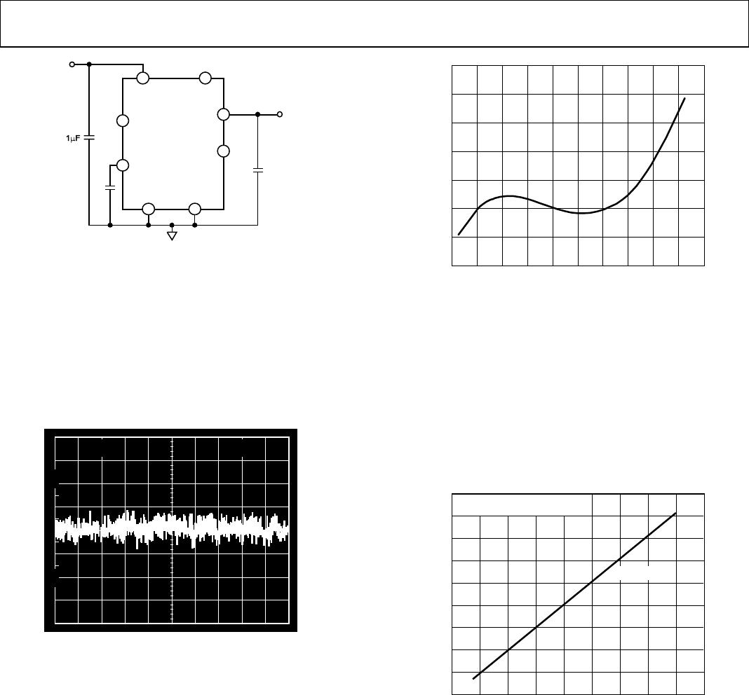
APPLYING THE AD780
The AD780 can be used without any external components to
achieve specified performance. If power is supplied to Pin 2 and
Pin 4 is grounded, Pin 6 provides a 2.5 V or 3.0 V output
depending on whether Pin 8 is left unconnected or grounded.
A bypass capacitor of 1 µF (+V
IN
to GND) should be used if the
load capacitance in the application is expected to be greater than
1 nF. The AD780 in 2.5 V mode typically draws 700 µA of I
q
at
5 V. This increases by ~2 µA/V up to 36 V.
00841-005
DNC
TEMP
+V
IN
R
NULL
V
OUT
TRIM
GND
O/P SELECT
2.5V – DNC
3.0V – GND
DNC
R POT
AD780
DNC = DO NOT CONNECT TO THIS PIN
1
7
6
5
84
2
3
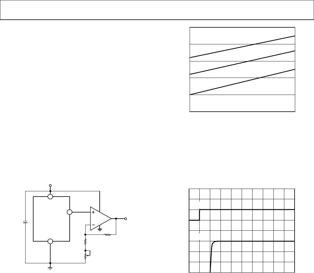
Figure 5. Optional Fine-Trim Circuit
Initial error can be nulled using a single 25 kΩ potentiometer
connected between V
OUT
, TRIM, and GND. This is a coarse trim
with an adjustment range of 4%, and is only included here for
compatibility purposes with other references. A fine trim can be
implemented by inserting a large value resistor (e.g., 1 MΩ to
5 MΩ) in series with the wiper of the potentiometer (see Figure 5).
The trim range, expressed as a fraction of the output, is simply
greater than or equal to 2.1 kΩ/R
NULL
for either the 2.5 V or
3.0 V mode.
The external null resistor affects the overall temperature
coefficient by a factor equal to the percentage of V
OUT
nulled.
For example, a 1 mV (0.03%) shift in the output caused by the
trim circuit, with a 100 ppm/°C null resistor, adds less than
0.06 ppm/°C to the output drift (0.03% × 200 ppm/°C, since the
resistors internal to the AD780 also have temperature coefficients
of less than 100 ppm/°C).
NOISE PERFORMANCE
The impressive noise performance of the AD780 can be further
improved, if desired, by adding two capacitors: a load capacitor
(C1) between the output and ground, and a compensation
capacitor (C2) between the TEMP pin and ground. Suitable
values are shown in Figure 6.
100
10
1
0.1
0.1 1 10 100
00841-006
LOAD CAPACITOR, C1 (µF)
COMPENSATION CAPACITOR, C2 (nF)
Figure 6. Compensation and Load Capacitor Combinations
C1 and C2 also improve the settling performance of the AD780
when subjected to load transients. The improvement in noise
performance is shown in Figure 7, Figure 8, Figure 9, and Figure 10.
00841-007
0.1 TO 10Hz
AMPLIFIER GAIN = 100
1s100µV
100
90
10
0%
Figure 7. Standalone Noise Performance
00841-008
10Hz TO 10kHz
NO AMPLIFIER
10ms20µV
100
90
10
0%
Figure 8. Standalone Noise Performance
Data Sheet AD780
Rev. H | Page 7 of 12
00841-009
DNC
TEMP
+V
IN
V
OUT
TRIM
GND
O/P SELECT
2.5V – DNC
3.0V – GND
DNC
AD780
DNC = DO NOT CONNECT TO THIS PIN
1
7
6
5
84
2
3
C2
C1
Figure 9. Noise Reduction Circuit
NOISE COMPARISON
The wideband noise performance of the AD780 can also be
expressed in ppm. The typical performance with C1 and C2 is
0.6 ppm; without external capacitors, typical performance is
1.2 ppm.
This performance is, respectively, 7× and 3× lower than the
specified performance of the LT1019.
00841-010
10Hz TO 10kHz
NO AMPLIFIER
10ms20µV
100
90
10
0%
Figure 10. Reduced Noise Performance with C1 = 100 µF, C2 = 100 nF
TEMPERATURE PERFORMANCE
The AD780 provides superior performance over temperature by
means of a combination of patented circuit design techniques,
precision thin-film resistors, and drift trimming. Temperature
performance is specified in terms of ppm/°C; because of
nonlinearity in the temperature characteristic, the box test
method is used to test and specify the part. The nonlinearity
takes the form of the characteristic S-shaped curve shown in
Figure 11. The box test method forms a rectangular box around
this curve, enclosing the maximum and minimum output voltages
over the specified temperature range. The specified drift is equal to
the slope of the diagonal of this box.
2.0
–0.8
–0.4
0
0.4
0.8
1.2
1.6
–60 –40 –20 0 20 40 60 80 100 120 140
00841-011
TEMPERATURE (°C)
ERROR (mV)
Figure 11. Typical AD780BN Temperature Drift
TEMPERATURE OUTPUT PIN
The AD780 provides a TEMP output (Pin 3) that varies linearly
with temperature. This output can be used to monitor changes
in system ambient temperature, and to initiate calibration of the
system, if desired. The voltage V
TEMP
is 560 mV at 25°C, and the
temperature coefficient is approximately 2 mV/°C.
Figure 12 shows the typical V
TEMP
characteristic curve over
temperature taken at the output of the op amp with a
noninverting gain of 5.
4.25
4.00
3.75
3.50
3.25
3.00
2.75
2.50
2.25
2.00
–75 –50 –25 0 25 50 75 100 125 150
00841-012
TEMPERATURE (°C)
VOLTAGE (V
OUT
)
CIRCUIT CALIBRATED AT 25°C
REFER TO FIGURE 13
10mV PER °C
Figure 12. Temperature Pin Transfer Characteristic
Since the TEMP voltage is acquired from the band gap core
circuit, current pulled from this pin has a significant effect on
V
OUT
. Care must be taken to buffer the TEMP output with a
suitable op amp, for example, an OP07, AD820, or AD711 (all
of which would result in less than a 100 µV change in V
OUT
).
The relationship between I
TEMP
and V
OUT
is
V
OUT
= 5.8 mV/µA I
TEMP
(2.5 V Range)
or
V
OUT
= 6.9 mV/µA I
TEMP
(3.0 V Range)
AD780 Data Sheet
Rev. H | Page 8 of 12
Notice how sensitive the current dependent factor on V
OUT
is. A
large amount of current, even in tens of microamps, drawn
from the TEMP pin can cause the V
OUT
and TEMP output to fail.
The choice of C1 and C2 was dictated primarily by the need for
a relatively flat response that rolled off early in the high frequency
noise at the output. However, there is considerable margin in
the choice of these capacitors. For example, the user can
actually put a huge C2 on the TEMP pin with none on the
output pin. However, one must either put very little or a lot of
capacitance at the TEMP pin. Intermediate values of capacitance
can sometimes cause oscillation. In any case, the user should
follow the recommendation in Figure 6.
TEMPERATURE TRANSDUCER CIRCUIT
The circuit shown in Figure 13 is a temperature transducer that
amplifies the TEMP output voltage by a gain of a little over +5 to
provide a wider full-scale output range. The digital potentiometer
can be used to adjust the output so it varies by exactly 10 mV/°C.
To minimize resistance changes with temperature, resistors with
low temperature coefficients, such as metal film resistors,
should be used.
00841-013
AD780
GND
R
B
1.27k
(1%)
R
F
6.04k
(1%)
4
+V
IN
2
3
1µ
F
TEMP
R
BP
200
AD820
10mV/°
C
5V
Figure 13. Differential Temperature Transducer
SUPPLY CURRENT OVER TEMPERATURE
The quiescent current of the AD780 varies slightly over
temperature and input supply range. The test limit is 1 mA over
the industrial and 1.3 mA over the military temperature range.
Typical performance with input voltage and temperature
variation is shown in Figure 14.
0.85
0.80
0.75
0.70
0.65
0.60
4
36
00841-014
INPUT VOLTAGE (V)
QUIESCENT CURRENT (mA)
–55°C
+25
°C
+125
°
C
Figure 14. Typical Supply Current over Temperature
TURN-ON TIME
The time required for the output voltage to reach its final value
within a specified error band is defined as the turn-on settling
time. The two major factors that affect this are the active circuit
settling time and the time for the thermal gradients on the chip
to stabilize. Typical settling performance is shown in Figure 15.
The AD780 settles to within 0.1% of its final value within 10 µs.
5V
0V
2.500V
2.499V
2.498V
00841-015
10µ
s/DIV
V
IN
V
OUT
Figure 15. Turn-On Settling Time Performance

AD780BR

Mfr. #:
Manufacturer:
Analog Devices Inc.
Description:
Voltage References 2.5V/3V Ultrahigh Prec Bandgap
Lifecycle:
New from this manufacturer.
Delivery:
DHL FedEx Ups TNT EMS
Payment:
T/T Paypal Visa MoneyGram Western Union