Data Sheet AD780
Rev. H | Page 3 of 12
SPECIFICATIONS
T
A
= 25°C, V
IN
= 5 V, unless otherwise noted.
Table 1.
AD780AN/AD780AR AD780CR AD780BN/AD780BR
Parameter Min Typ Max Min Typ Max Min Typ Max Unit
OUTPUT VOLTAGE
2.5 V Out 2.495 2.505 2.4985 2.5015 2.499 2.501 V
3.0 V Out 2.995 3.005 2.9950 3.0050 2.999 3.001 V
SOLDER HEAT SHIFT
Mean −1.1 −1.1 −1.1 mV
Sigma 0.4 0.4 0.4 mV
OUTPUT VOLTAGE DRIFT
1
−40°C to +85°C 7 7 3 ppm/°C
−55°C to +125°C 20 20 ppm/°C
LINE REGULATION
2.5 V Output, 4 V ≤+V
IN
36 V, T
MIN
to T
MAX
10 10 10 µV/V
3.0 V Output, 4.5 V ≤+V
IN
36 V, T
MIN
to T
MAX
10 10 10 µV/V
LOAD REGULATION, SERIES MODE
Sourcing 0 mA < I
OUT
< 10 mA 50 50 50 µV/mA
T
MIN
to T
MAX
75 75 75 µV/mA
Sinking −10 mA < I
OUT
< 0 mA 75 75 75 µV/mA
−40°C to +85°C 75 75 75 µV/mA
−55°C to +125°C 150 150 150 µV/mA
LOAD REGULATION, SHUNT MODE
I < I
SHUNT
< 10 mA 75 75 75 µV/mA
QUIESCENT CURRENT, 2.5 V SERIES MODE
2
40°C to +85°C
0.75
1.0
0.75
1.0
0.75
1.0
mA
−55°C to +125°C 0.8 1.3 0.8 1.3 0.8 1.3 mA
MINIMUM SHUNT CURRENT 0.7 1.0 0.7 1.0 0.7 1.0 mA
OUTPUT NOISE
0.1 Hz to 10 Hz 4 4 4 µV p-p
Spectral Density, 100 Hz 100 100 100
nV/√
Hz
LONG-TERM STABILITY
3
20 20 20 ± ppm/1000 Hr
TRIM RANGE 4.0 4.0 4.0 ± %
TEMPERATURE PIN
Voltage Output @ 25°C
560
620
500
560
620
500
560
620
mV
Temperature Sensitivity 1.9 1.9 1.9 mV/°C
Output Resistance 3 3 3 kΩ
SHORT-CIRCUIT CURRENT TO GROUND 30 30 30 mA
TEMPERATURE RANGE
Specified Performance (A, B, C)
+85
−40
+85
−40
+85
°C
Operating Performance (A, B, C)
4
−55 +125 −55 +125 −55 +125 °C
1
Maximum output voltage drift is guaranteed for all packages.
2
3.0 V mode typically adds 100 µA to the quiescent current. Also, Iq increases by 2 µA/V above an input voltage of 5 V.
3
The long-term stability specification is noncumulative. The drift in subsequent 1,000 hour periods is significantly lower than in the first 1,000 hour period.
4
The operating temperature range is defined as the temperature extremes at which the device will still function. Parts may deviate from their specified performance
outside their specified temperature range.
AD780 Data Sheet
Rev. H | Page 4 of 12
ABSOLUTE MAXIMUM RATINGS
Table 2.
Parameter Values
+V
IN
to Ground 36 V
TRIM Pin to Ground 36 V
TEMP Pin to Ground 36 V
Power Dissipation (25°C) 500 mW
Storage Temperature −65°C to +150°C
Lead Temperature
(Soldering 10 sec)
300°C
Output Protection
Output safe for indefinite short to
ground and momentary short to V
IN
.
ESD Classification Class 1 (1000 V)
Stresses at or above those listed under Absolute Maximum
Ratings may cause permanent damage to the product. This is a
stress rating only; functional operation of the product at these
or any other conditions above those indicated in the operational
section of this specification is not implied. Operation beyond
the maximum operating conditions for extended periods may
affect product reliability.
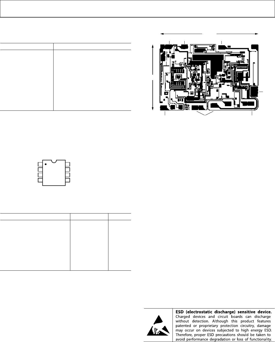
00841-002
NOTES
1. DNC = DO NOT CONNECT T
O THIS PIN.
AD780
TOP
VIEW
(Not to Scale)
DNC
1
+V
IN
2
TEMP
3
GND
4
2.5V/3.0V O/PSELECT
(DNC OR GND)
DNC
V
OUT
TRIM
8
7
6
5
Figure 2. Pin Configuration, 8-Lead PDIP and SOIC Packages
Table 3. Die Physical Characteristics
Parameter Value Units
Die Size 67 × 96 mil
Back Grind Thickness 10 mil
Bond Pad Opening Size 89 × 136 µm
Top Metal Composition
AlCu (0.5%)
%
Passivation Oxynitride
Polyimide None µm
Die Marker 780
Substrate Bias GND V
00841-003
GND
TEMP
96 mils
67 mils
+V
IN
TRIM 2.5V/3.0V
O/P SELECT
V
OUT
GND
Figure 3. Die Layout
NOTES
Both V
OUT
pads must be connected to the output.
Die Thickness: The standard thickness of Analog Devices, Inc.
bipolar dice is 10 mil ± 1 mil.
Die Dimensions: The dimensions given are the maximum possible
die size.
Backing: The standard backside surface is silicon (not plated).
Analog Devices does not recommend gold-backed dice for most
applications.
Edges: A diamond saw is used to separate wafers into dice, thus
providing perpendicular edges halfway through the die. In
contrast to scribed dice, this technique provides a more uniform
die shape and size. The perpendicular edges facilitate handling
(such as tweezer pickup), while the uniform shape and size
simplify substrate design and die attach.
Top Surface: The standard top surface of the die is covered by a
layer of passivation. All areas are covered except bonding pads
and scribe lines.
Surface Metallization: The metallization to Analog Devices
bipolar dice is aluminum/copper. The minimum thickness is
10,000 Å.
Bonding Pads: All bonding pads have a minimum size of
4.0 mil by 6.0 mil. The passivation windows have a minimum
size of 3.5 mil by 5.3 mil.
ESD CAUTION
Data Sheet AD780
Rev. H | Page 5 of 12
THEORY OF OPERATION
Band gap references are the high performance solution for low
supply voltage and low power voltage reference applications. In
this technique, a voltage with a positive temperature coefficient
is combined with the negative coefficient of a transistor’s V
be
to
produce a constant band gap voltage.
In the AD780, the band gap cell contains two NPN transistors
(Q6 and Q7) that differ in emitter area by 12×. The difference in
their V
be
s produces a PTAT current in R5. This, in turn, produces a
PTAT voltage across R4 that, when combined with the V
be
of
Q7, produces a voltage (V
bg
) that does not vary with temperature.
Precision laser trimming of the resistors and other patented circuit
techniques are used to further enhance the drift performance.
00841-004
R16
R10
+V
IN
R4
R5
Q6
Q7
R
11
R14
R13
R15
DNC
V
OUT
TRIM
GND
O/P SELECT
2.5V – NC
3.0V – GND
TEMP
DNC
DNC = DO NOT CONNECT T
O THIS PIN
AD780
72
1
3
4 8
5
6
Figure 4. Schematic Diagram
The output voltage of the AD780 is determined by the
configuration of Resistors R13, R14, and R15 in the amplifier’s
feedback loop. This sets the output to either 2.5 V or 3.0 V,
depending on whether R15 (Pin 8) is grounded or not connected.
A unique feature of the AD780 is the low headroom design of
the high gain amplifier, which produces a precision 3 V output
from an input voltage as low as 4.5 V (or 2.5 V from a 4.0 V
input). The amplifier design also allows the part to work with
+V
IN
= V
OUT
when current is forced into the output terminal.
This allows the AD780 to work as a 2-terminal shunt regulator,
providing a −2.5 V or −3.0 V reference voltage output without
external components.
The PTAT voltage is also used to provide the user with a
thermometer output voltage (at Pin 3) that increases at a rate of
approximately 2 mV/°C.
The DNC (Pin 7) of the AD780 is a 20 kΩ resistor to +V
IN
that
is used solely for production test purposes. Users who are currently
using the LT1019 self-heater pin (Pin 7) must take into account
the different load on the heater supply.

AD780BR

Mfr. #:
Manufacturer:
Analog Devices Inc.
Description:
Voltage References 2.5V/3V Ultrahigh Prec Bandgap
Lifecycle:
New from this manufacturer.
Delivery:
DHL FedEx Ups TNT EMS
Payment:
T/T Paypal Visa MoneyGram Western Union