Data Sheet AD780
Rev. H | Page 9 of 12
DYNAMIC PERFORMANCE
The output stage of the AD780 has been designed to provide
superior static and dynamic load regulation.
Figure 16 and Figure 17 show the performance of the AD780
while driving a 0 mA to 10 mA load.
00841-016
AD780
4
+V
IN
2
6
1µF
V
OUT
249
V
L
V
OUT
0V
Figure 16. Transient Resistive Load Test Circuit
0mA
10mA
00841-017
10µs/DIV
OUTPUT CHANGE (50mV/DIV)
I
LOAD
V
OUT
(C
L
= 0pF)
Figure 17. Settling Under Transient Resistive Load
The dynamic load may be resistive and capacitive. For example,
the load may be connected via a long capacitive cable. Figure 18
and Figure 19 show the performance of the AD780 driving a
1000 pF, 0 mA to 10 mA load.
00841-018
AD780
4
+V
IN
2
6
1µ
F
V
OUT
249
V
L
V
OUT
0V
C
L
1000pF
Figure 18. Capacitive Load Transient Response Test Circuit
0mA
10mA
00841-019
10µs/DIV
OUTPUT CHANGE (50mV/DIV)
I
LOAD
V
OUT
(C
L
= 1000pF)
Figure 19. Settling under Dynamic Capacitive Load
LINE REGULATION
Line regulation is a measure of change in output voltage due to
a specified change in input voltage. It is intended to simulate
worst-case unregulated supply conditions and is measured in
µV/V. Figure 20 shows typical performance with 4.0 V < V
IN
<
15.0 V.
200
100
0
–100
–200
4 1510
00841-020
INPUT VOLTAGE (V)
OUTPUT CHANGE (µV)
T = 25°C
Figure 20. Output Voltage Change vs. Input Voltage
AD780 Data Sheet
Rev. H | Page 10 of 12
PRECISION REFERENCE FOR HIGH RESOLUTION
5 V DATA CONVERTERS
The AD780 is ideally suited to be the reference for most 5 V
high resolution ADCs. The AD780 is stable under any capacitive
load, has superior dynamic load performance, and its 3.0 V
output provides the converter with the maximum dynamic
range without requiring an additional and expensive buffer
amplifier. One of the many ADCs that the AD780 is suited for is
the AD7884, a 16-bit, high speed sampling ADC (see Figure 21).
This part previously needed a precision 5 V reference, resistor
divider, and buffer amplifier to do this function.
00841-021
+V
IN
AD780
AD7884
V
OUT
V
REF
+ F
6
V
REF
+ S
2.5V/3.0V
SELECT
8
GND
4
2
1µF
5V
Figure 21. Precision 3 V Reference for the AD7884 16-Bit, High Speed ADC
The AD780 is also ideal for use with higher resolution converters,
such as the AD7710/AD7711/AD7712 (see Figure 22. While these
parts are specified with a 2.5 V internal reference, the AD780 in
3 V mode can be used to improve the absolute accuracy,
temperature stability, and dynamic range. It is shown in Figure 22
with the two optional noise reduction capacitors.
00841-022
+V
IN
AD780
AD7710
V
OUT
REF IN+
6
2.5V/3.0V
O/P SELECT
8
GND
4
3
2
1µF
100nF
5V
REF IN–
100µF
Figure 22. Precision 2.5 V or 3.0 V Reference for the
AD7710 High Resolution, Σ-Δ ADC
4.5 V REFERENCE FROM 5 V SUPPLY
Some 5 V high resolution ADCs can accommodate reference
voltages up to 4.5 V. The AD780 can be used to provide a
precision 4.5 V reference voltage from a 5 V supply using the
circuit shown in Figure 23. This circuit provides a regulated
4.5 V output from a supply voltage as low as 4.7 V. The high
quality tantalum 10 µF capacitor, in parallel with the ceramic
AD780 0.1 µF capacitor and the 3.9 Ω resistor, ensures a low
output impedance around 50 MHz.
00841-023
AD780
2N2907
V
OUT
5k
0.01%
4k
0.01%
2.5k
3.9
1k
0.1µF
0.1µF
10µF
0.1µF
OP90
+
V
SUPPLY
2
4
6
3
7
6
4
2
Figure 23. 4.5 V Reference from a Single 5 V Supply
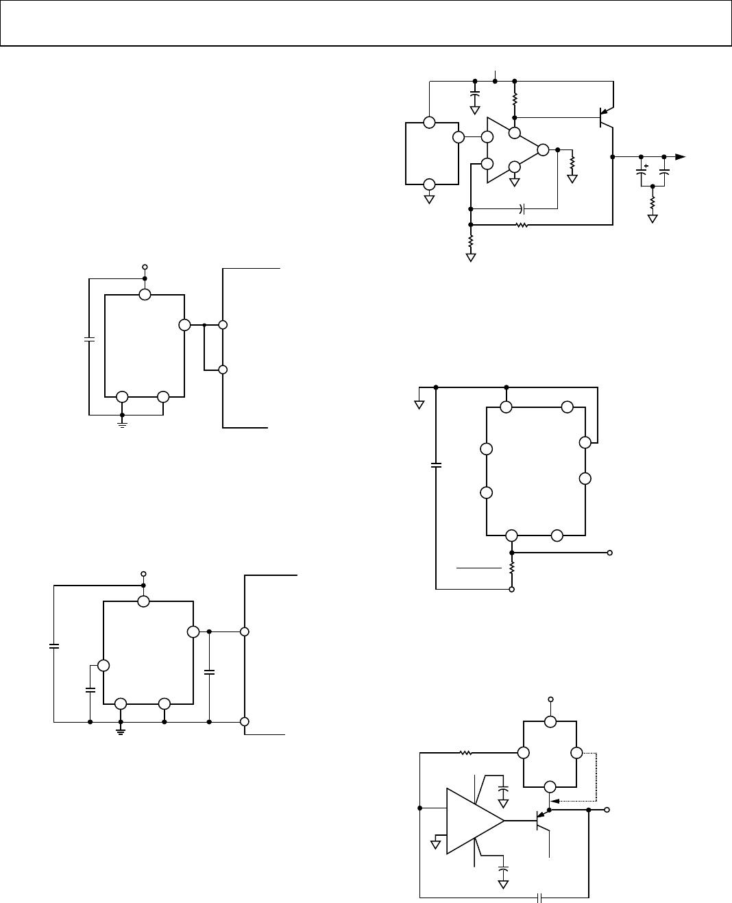
NEGATIVE (2.5 V) REFERENCE
The AD780 can produce a negative output voltage in shunt mode
by connecting the input and output to ground, and connecting
the GND pin of the AD780 to a negative supply via a bias resistor,
as shown in Figure 25.
00841-024
DNC
TEMP
1µF
+V
IN
V
OUT
TRIM
GND
O/P SELECT
2.5V – DNC
3.0V – GND
DNC
AD780
NOTES
1. I
L
= LOAD CURRENT
2. I
S
MIN = MINIMUM SHUNT CURRENT
3. DNC = DO NOT CONNECT TO THIS PIN
1
7
6
5
84
2
3
R =
V
OUT
– (V–)
I
L
+ I
S
MIN
–2.5 V
OUT
V–
Figure 24. Negative (−2.5 V Shunt Mode Reference)
A precise 2.5 V reference capable of supplying up to 100 mA to
a load can be implemented with the AD780 in series mode, using
the bootstrap circuit shown in Figure 25.
00841-025
AD780
2N3906
+5V
+5V
OP07
CONNECT IF
–3V OUTPUT
DESIRED
–2.5V (I
L
100mA)
–5V
–5V
OUT
1k
1000pF
+V
IN
+
2
4
6 8
Figure 25. −2.5 V High Load Current Reference
Data Sheet AD780
Rev. H | Page 11 of 12
OUTLINE DIMENSIONS
CONTROLLING DIMENSIONS ARE IN MILLIMETERS; INCH DIMENSIONS
(IN PARENTHESES) ARE ROUNDED-OFF MILLIMETER EQUIVALENTS FOR
REFERENCE ONLY AND ARE NOT APPROPRIATE FOR USE IN DESIGN.
COMPLIANT TO JEDEC STANDARDS MS-012-AA
012407-A
0.25 (0.0098)
0.17 (0.0067)
1.27 (0.0500)
0.40 (0.0157)
0.50 (0.0196)
0.25 (0.0099)
45°
1.75 (0.0688)
1.35 (0.0532)
SEATING
PLANE
0.25 (0.0098)
0.10 (0.0040)
4
1
8 5
5.00 (0.1968)
4.80 (0.1890)
4.00 (0.1574)
3.80 (0.1497)
1.27 (0.0500)
BSC
6.20 (0.2441)
5.80 (0.2284)
0.51 (0.0201)
0.31 (0.0122)
COPLANARITY
0.10
Figure 26. 8-Lead Standard Small Outline Package [SOIC_N]
Narrow Body (R-8)
Dimensions shown in millimeters and (inches)
COMPLIANT TO JEDEC STANDARDS MS-001
CONTROLLING DIMENSIONSARE IN INCHES; MILLIMETER DIMENSIONS
(IN PARENTHESES) ARE ROUNDED-OFF INCH EQUIVALENTS FOR
REFERENCE ONLY AND ARE NOT APPROPRIATE FOR USE IN DESIGN.
CORNER LEADS MAY BE CONFIGURED AS WHOLE OR HALF LEADS.
070606-A
0.022 (0.56)
0.018 (0.46)
0.014 (0.36)
SEATING
PLANE
0.015
(0.38)
MIN
0.210 (5.33)
MAX
0.150 (3.81)
0.130 (3.30)
0.115 (2.92)
0.070 (1.78)
0.060 (1.52)
0.045 (1.14)
8
1
4
5
0.280 (7.11)
0.250 (6.35)
0.240 (6.10)
0.100 (2.54)
BSC
0.400 (10.16)
0.365 (9.27)
0.355 (9.02)
0.060 (1.52)
MAX
0.430 (10.92)
MAX
0.014 (0.36)
0.010 (0.25)
0.008 (0.20)
0.325 (8.26)
0.310 (7.87)
0.300 (7.62)
0.195 (4.95)
0.130 (3.30)
0.115 (2.92)
0.015 (0.38)
GAUGE
PLANE
0.005 (0.13)
MIN
Figure 27. 8-Lead Plastic Dual-In-Line Package [PDIP]
Narrow Body
(N-8)
Dimensions shown in inches and (millimeters)

AD780BR

Mfr. #:
Manufacturer:
Analog Devices Inc.
Description:
Voltage References 2.5V/3V Ultrahigh Prec Bandgap
Lifecycle:
New from this manufacturer.
Delivery:
DHL FedEx Ups TNT EMS
Payment:
T/T Paypal Visa MoneyGram Western Union