© 2008 Microchip Technology Inc. DS22062B-page 1
MCP14E3/MCP14E4/MCP14E5
Features
High Peak Output Current: 4.0A (typical)
Independent Enable Function for Each Driver
Output
Low Shoot-Through/Cross-Conduction Current in
Output Stage
Wide Input Supply Voltage Operating Range:
- 4.5V to 18V
High Capacitive Load Drive Capability:
- 2200 pF in 15 ns (typical)
- 5600 pF in 26 ns (typical)
Short Delay Times: 50 ns (typical)
Latch-Up Protected: Will Withstand 1.5A Reverse
Current
Logic Input Will Withstand Negative Swing Up To
5V
Space-Saving Packages:
- 8-Lead 6x5 DFN, PDIP, SOIC
Applications
Switch Mode Power Supplies
Pulse Transformer Drive
Line Drivers
Motor and Solenoid Drive
General Description
The MCP14E3/MCP14E4/MCP14E5 devices are a
family of 4.0A buffers/MOSFET drivers. Dual-inverting,
dual-noninvertering, and complementary outputs are
standard logic options offered.
The MCP14E3/MCP14E4/MCP14E5 drivers are
capable of operating from a 4.5V to 18V single power
supply and can easily charge and discharge 2200 pF
gate capacitance in under 15 ns (typical). They provide
low impedance in both the ON and OFF states to
ensure the MOSFET’s intended state will not be
affected, even by large transients. The MCP14E3/
MCP14E4/MCP14E5 inputs may be driven directly
from either TTL or CMOS (2.4V to 18V).
Additional control of the MCP14E3/MCP14E4/
MCP14E5 outputs is allowed by the use of separate
enable functions. The ENB_A and ENB_B pins are
active high and are internally pulled up to V
DD
. The pins
maybe left floating for standard operation.
The MCP14E3/MCP14E4/MCP14E5 dual-output 4.0A
driver family is offered in both surface-mount and pin-
through-hole packages with a -40°C to +125°C
temperature rating. The low thermal resistance of the
thermally enhanced DFN package allows for greater
power dissipation capability for driving heavier
capacitive or resistive loads.
These devices are highly latch-up resistant under any
conditions within their power and voltage ratings. They
are not subject to damage when up to 5V of noise
spiking (of either polarity) occurs on the ground pin.
They can accept, without damage or logic upset, up to
1.5A of reverse current being forced back into their
outputs. All terminals are fully protect against
Electrostatic Discharge (ESD) up to 4 kV.
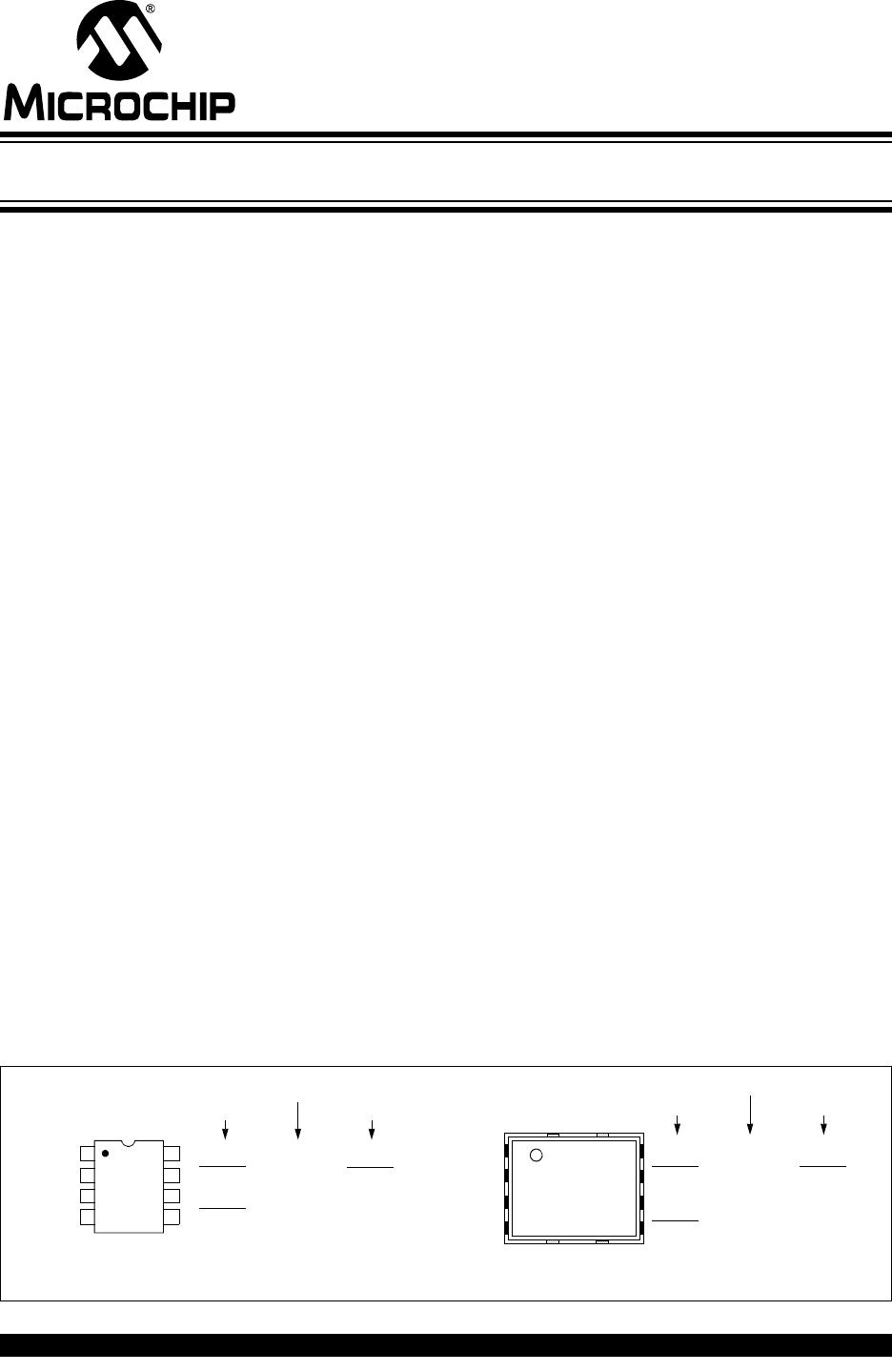
Package Types
ENB_A
IN A
GND
IN B
8-Pin
1
2
3
4
ENB_B
5
6
7
8
OUT A
OUT B
ENB_A
IN A
GND
IN B
V
DD
Note 1: Exposed pad of the DFN package is electrically isolated.
MCP14E3
MCP14E4
ENB_B
OUT A
OUT B
V
DD
MCP14E5
ENB_B
OUT A
OUT B
V
DD
ENB_B
OUT A
OUT B
V
DD
MCP14E3
MCP14E4
ENB_B
OUT A
OUT B
V
DD
MCP14E5
ENB_B
OUT A
OUT B
V
DD
PDIP/SOIC
8-Pin
6x5 DFN
(1)
1
2
3
4
5
6
7
8
4.0A Dual High-Speed Power MOSFET Drivers With Enable
MCP14E3/MCP14E4/MCP14E5
DS22062B-page 2 © 2008 Microchip Technology Inc.
Functional Block Diagram
Effective
Input C = 20 pF
(Each Input)
MCP14E3
MCP14E4
MCP14E5
Dual Inverting
Dual Noninverting
One Inverting, One Noninverting
Output
Input
GND
V
DD
4.7 V
Inverting
Non-inverting
Enable
V
DD
Internal
Pull-up
4.7 V
© 2008 Microchip Technology Inc. DS22062B-page 3
MCP14E3/MCP14E4/MCP14E5
1.0 ELECTRICAL
CHARACTERISTICS
Absolute Maximum Ratings †
Supply Voltage................................................................+20V
Input Voltage...............................(V
DD
+ 0.3V) to (GND – 5V)
Enable Voltage.............................(V
DD
+ 0.3V) to (GND - 5V)
Input Current (V
IN
>V
DD
)................................................50 mA
Package Power Dissipation (T
A
= 50°C)
8L-DFN ....................................................................... Note 3
8L-PDIP ........................................................................1.10W
8L-SOIC.....................................................................665 mW
Notice: Stresses above those listed under "Maximum
Ratings" may cause permanent damage to the device. This is
a stress rating only and functional operation of the device at
those or any other conditions above those indicated in the
operational sections of this specification is not intended.
Exposure to maximum rating conditions for extended periods
may affect device reliability.
DC CHARACTERISTICS (NOTE 2)
Electrical Specifications: Unless otherwise indicated, T
A
= +25°C, with 4.5V V
DD
18V.
Parameters Sym Min Typ Max Units Conditions
Input
Logic ‘1’, High Input Voltage V
IH
2.4 1.5 V
Logic ‘0’, Low Input Voltage V
IL
—1.30.8V
Input Current I
IN
–1 1 µA 0VV
IN
V
DD
Input Voltage V
IN
-5 V
DD
+0.3 V
Output
High Output Voltage V
OH
V
DD
– 0.025 V DC Test
Low Output Voltage V
OL
0.025 V DC Test
Output Resistance, High R
OH
—2.53.5Ω I
OUT
= 10 mA, V
DD
= 18V
Output Resistance, Low R
OL
—2.53.0Ω I
OUT
= 10 mA, V
DD
= 18V
Peak Output Current I
PK
—4.0AV
DD
= 18V (Note 2)
Latch-Up Protection With-
stand Reverse Current
I
REV
>1.5 A Duty cycle2%, t 300 µs
Switching Time (Note 1)
Rise Time t
R
—1530nsFigure 4-1, Figure 4-2
C
L
= 2200 pF
Fall Time t
F
—1830nsFigure 4-1, Figure 4-2
C
L
= 2200 pF
Propagation Delay Time t
D1
—4655nsFigure 4-1, Figure 4-2
Propagation Delay Time t
D2
—5055nsFigure 4-1, Figure 4-2
Enable Function (ENB_A, ENB_B)
High-Level Input Voltage V
EN_H
1.60 1.90 2.90 V V
DD
= 12V, LO to HI Transition
Low-Level Input Voltage V
EN_L
1.30 2.20 2.40 V V
DD
= 12V, HI to LO Transition
Hysteresis V
HYST
0.10 0.30 0.60 V
Enable Leakage Current I
ENBL
40 85 115 µA V
DD
=12V,
ENB_A = ENB_B = GND
Propagation Delay Time t
D3
—60nsFigure 4-3 (Note 1)
Propagation Delay Time t
D4
—50nsFigure 4-3 (Note 1)
Note 1: Switching times ensured by design.
2: Tested during characterization, not production tested.
3: Package power dissipation is dependent on the copper pad area on the PCB.

MCP14E5-E/MF

Mfr. #:
Manufacturer:
Microchip Technology
Description:
Gate Drivers 45A Dual MOSFET Driver
Lifecycle:
New from this manufacturer.
Delivery:
DHL FedEx Ups TNT EMS
Payment:
T/T Paypal Visa MoneyGram Western Union