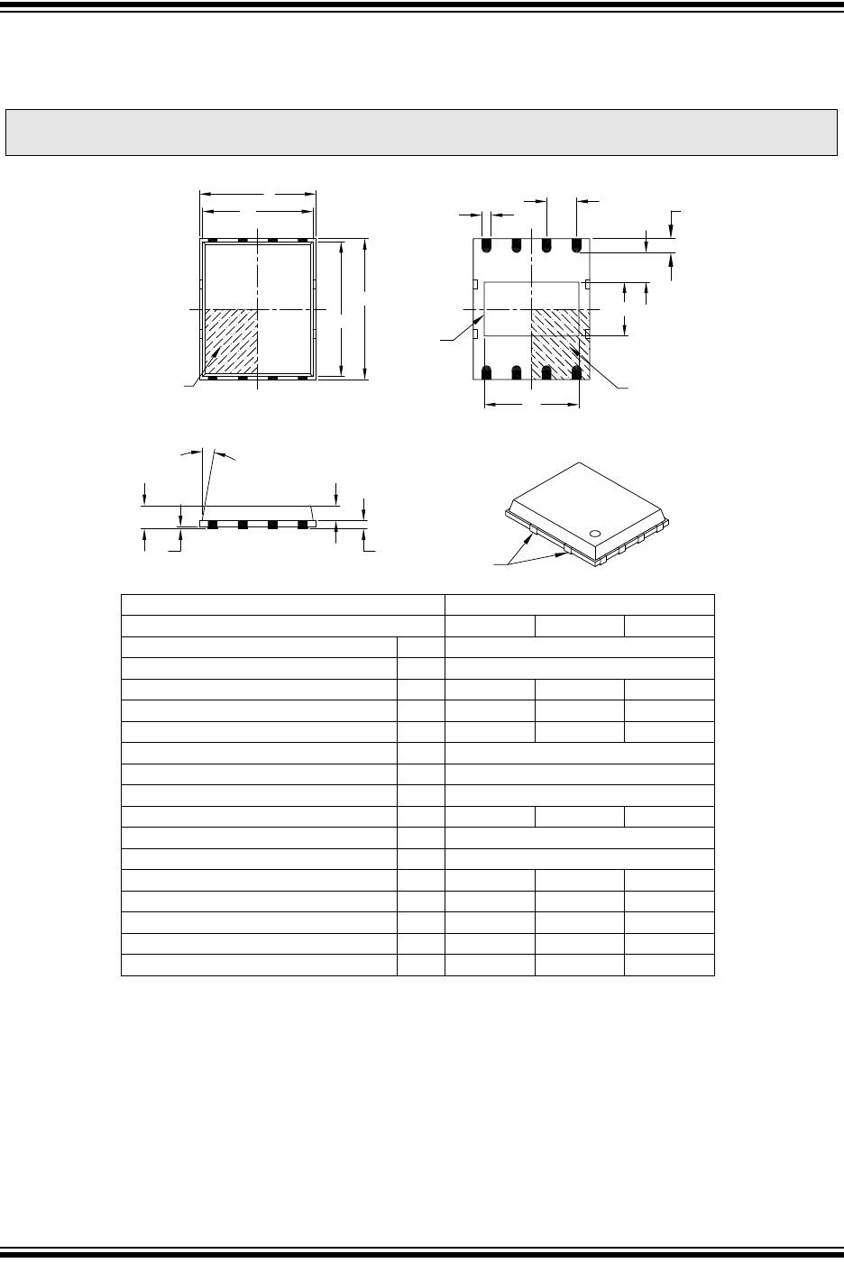
8-Lead Plastic Dual Flat, No Lead Package (MF) – 6x5 mm Body [DFN-S]
PUNCH SINGULATED
Notes:
1. Pin 1 visual index feature may vary, but must be located within the hatched area.
2. Package may have one or more exposed tie bars at ends.
3. Dimensioning and tolerancing per ASME Y14.5M.
BSC: Basic Dimension. Theoretically exact value shown without tolerances.
REF: Reference Dimension, usually without tolerance, for information purposes only.
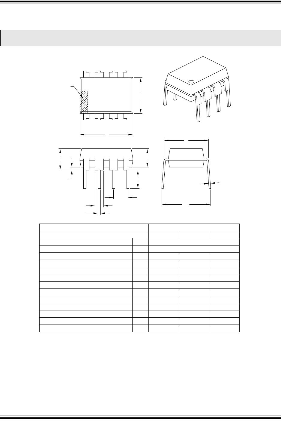
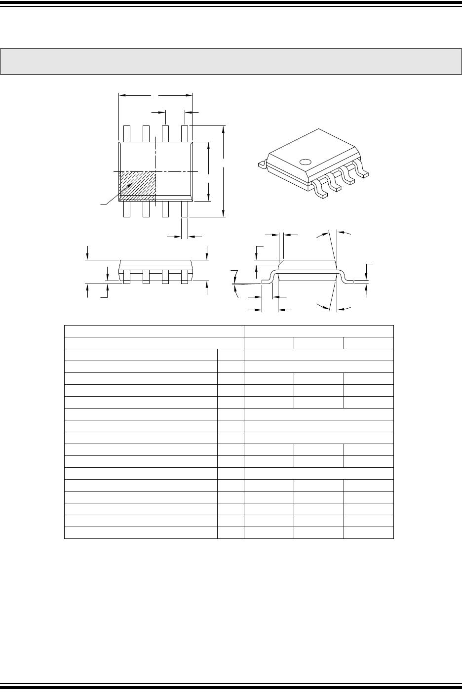
Note: For the most current package drawings, please see the Microchip Packaging Specification located at
http://www.microchip.com/packaging
Units MILLIMETERS
Dimension Limits MIN NOM MAX
Number of Pins N 8
Pitch e 1.27 BSC
Overall Height A – 0.85 1.00
Molded Package Thickness A2 – 0.65 0.80
Standoff A1 0.00 0.01 0.05
Base Thickness A3 0.20 REF
Overall Length D 4.92 BSC
Molded Package Length D1 4.67 BSC
Exposed Pad Length D2 3.85 4.00 4.15
Overall Width E 5.99 BSC
Molded Package Width E1 5.74 BSC
Exposed Pad Width E2 2.16 2.31 2.46
Contact Width b 0.35 0.40 0.47
Contact Length L 0.50 0.60 0.75
Contact-to-Exposed Pad K 0.20 – –
Model Draft Angle Top φ – – 12°
φ
NOTE 2
A3
A2
A1
A
NOTE 1
NOTE 1
EXPOSED
PAD
BOTTOM VIEW
1
2
D2
2
1
E2
K
L
N
e
b
E
E1
D
D1
N
TOP VIEW
Microchip Technology Drawing C04-113B