General Description
The MAX6974/MAX6975 precision current-sinking,
24-output PWM LED drivers drive red, green, and blue
LEDs for full-color graphic message boards and video
displays. Each output has an individual 12-bit (MAX6974)
or 14-bit (MAX6975) PWM-intensity (hue) control and
7-bit (MAX6974) or 5-bit (MAX6975) global PWM intensity
(luminance) control. The MAX6974/MAX6975 feature a
high-speed, fully buffered cascadable serial interface,
open-circuit LED fault detection circuitry, as well as a
watchdog timer.
The driver has three banks of eight outputs, with each
bank intended to drive a different color in RGB applica-
tions. The full-scale current for each bank of eight out-
puts is adjustable from 6mA to 30mA in 256 steps
(0.3125% per step) to calibrate each color.
The MAX6974/MAX6975 can optionally multiplex by
using outputs MUX0 and MUX1, which each drive an
external pnp transistor. Multiplexing doubles the
MAX6974/MAX6975 drive capability to 48 LEDs.
The MAX6974/MAX6975 operate from a 3.0V to 3.6V
power supply. The LED power supply can range from
3V to 7V. The LED drivers require only 0.8V headroom
above the LEDs’ forward-voltage drop. Using a sepa-
rate LED supply voltage for each LED minimizes power
consumption.
The serial interface uses differential signaling for the
high-speed clock and data signals to reduce EMI and
improve signal integrity. The MAX6974/MAX6975 buffer
all interface signals to simplify cascading devices in
modules that use a large number of drivers.
An internal watchdog timer, when enabled, automatically
clears the pixel-data registers and blanks the display if
any of the signal inputs fail to toggle within 40ms.
The MAX6974/MAX6975 are available in 40-pin TQFN
packages and operate over the -40°C to +125°C
temperature range.
Refer to the MAX6972/MAX6973 data sheet for a
16-output, 11mA to 55mA software-compatible device.
Applications
LED Video Display Panels
LED Message Boards
Variable Message Signs (VMS)
Signs
Graphic Panels
Features
24 LED Current Sink Outputs (Three Banks of
Eight Outputs)
48 LED Drive Option When Multiplexing
33MHz Clock Supports Up to 63 Frames per
Second of Video
Constant Output Current Calibration from 6mA to
30mA in 256 Steps
EZCascade™ Interface Simplifies Multiple Driver
Cascading Without External Buffers
12-Bit or 14-Bit Individual PWM LED Intensity
Controls
7-Bit or 5-Bit Panel PWM-Intensity Control
+3V to +7V LED Power Supply
+3.0V to +3.6V Logic Supply
Open-Circuit LED Fault Detection
Optional Watchdog Timer Blanks Display if
Interface Fails
Standard -40°C to +125°C Operating Temperature
Range
MAX6974/MAX6975
24-Output PWM LED Drivers
for Message Boards
________________________________________________________________
Maxim Integrated Products
1
19-0555; Rev 2; 10/07
For pricing, delivery, and ordering information, please contact Maxim Direct at 1-888-629-4642,
or visit Maxim’s website at www.maxim-ic.com.
EVALUATION KIT
AVAILABLE
Typical Operating Circuit appears at the end of data sheet.
*
EP = Exposed paddle.
+
Denotes a lead-free package.
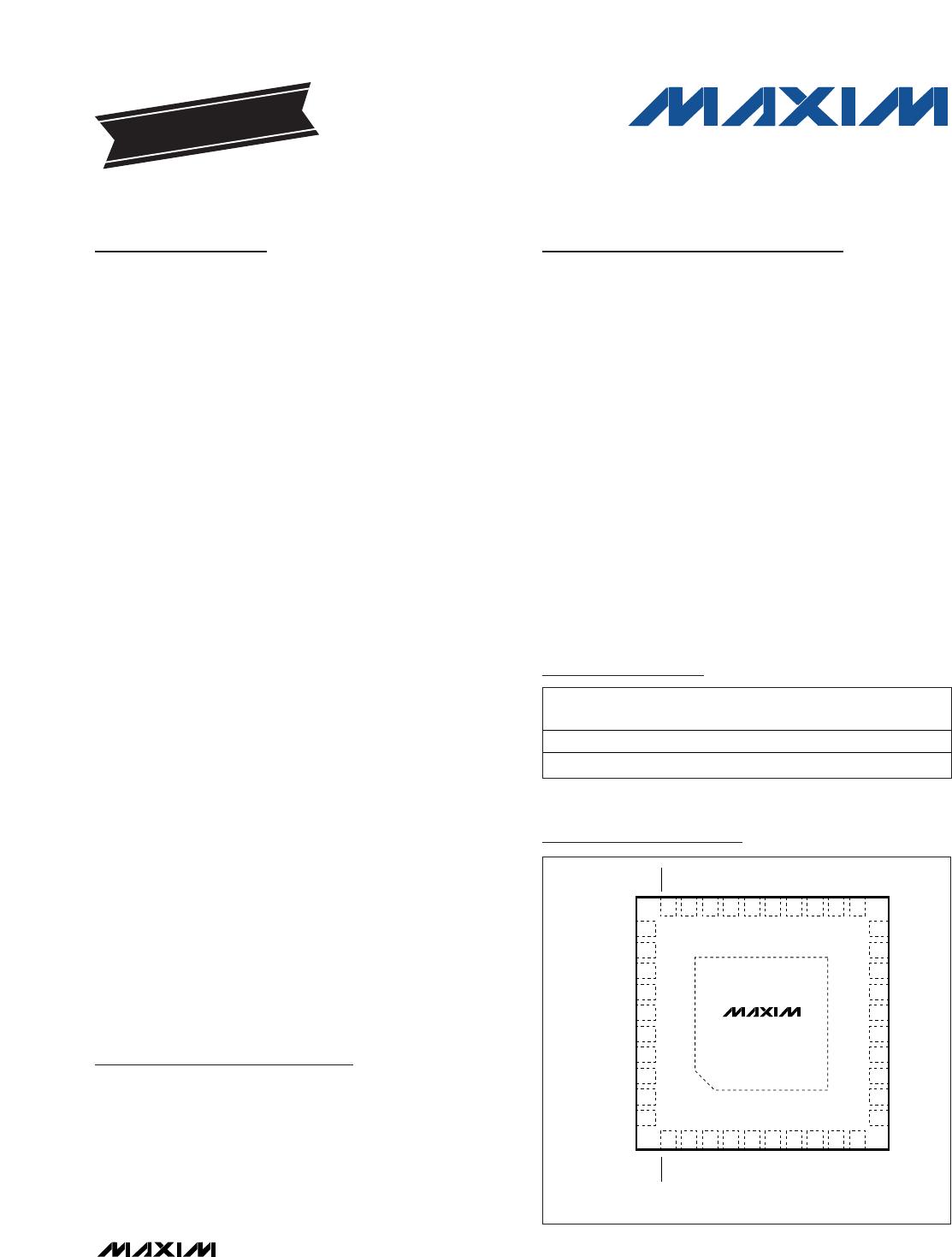
MAX6974ATL/
MAX6975ATL
TQFN-EP
TOP VIEW
35
36
34
33
12
11
13
14
12
+
B5
4567
2728
EP*
*EP = EXPOSED PADDLE.
2930 26 24 23 22
B4
B3
G2
G1
G0
R7
3
25
37
B2
R6
38
39
40
B1
B0
V
DD
R5
R4
R3
B6
32
15
G3
B7
31
16
17
18
19
20
G4
8910
21
AGND
R2
R1
R0
I.C.
LOADI
DIN-
DIN+
CLKI-
CLKI+
MUX0
CLKO+
CLK0-
DOUT+
DOUT-
LOADO
V
DD
G7
G6
G5
MUX1
Pin Configuration
Ordering Information
PART
TEMP RANGE
PIN-
PACKAGE
PKG
CODE
MAX6974ATL+ -40°C to +125°C 40 TQFN-EP*
T4066-3
MAX6975ATL+ -40°C to +125°C 40 TQFN-EP*
T4066-3
EZCascade is a trademark of Maxim Integrated Products, Inc.
MAX6974/MAX6975
24-Output PWM LED Drivers
for Message Boards
2 _______________________________________________________________________________________
ABSOLUTE MAXIMUM RATINGS
Stresses beyond those listed under “Absolute Maximum Ratings” may cause permanent damage to the device. These are stress ratings only, and functional
operation of the device at these or any other conditions beyond those indicated in the operational sections of the specifications is not implied. Exposure to
absolute maximum rating conditions for extended periods may affect device reliability.
(All voltages with respect to GND.)
V
DD
........................................................................-0.3V to +4.0V
R0–R7, G0–G7, B0–B7, MUX0, and MUX1 ...........-0.3V to +8.0V
All Other Pins..............................................-0.3V to (V
DD
+ 0.3V)
Continuous Power Dissipation (T
A
= +70°C)
40-Pin TQFN (derate 37mW/°C over +70°C) .............2963mW
Operating Temperature Range .........................-40°C to +125°C
Junction Temperature......................................................+150°C
Storage Temperature Range .............................-65°C to +150°C
Lead Temperature (soldering, 10s) .................................+300°C
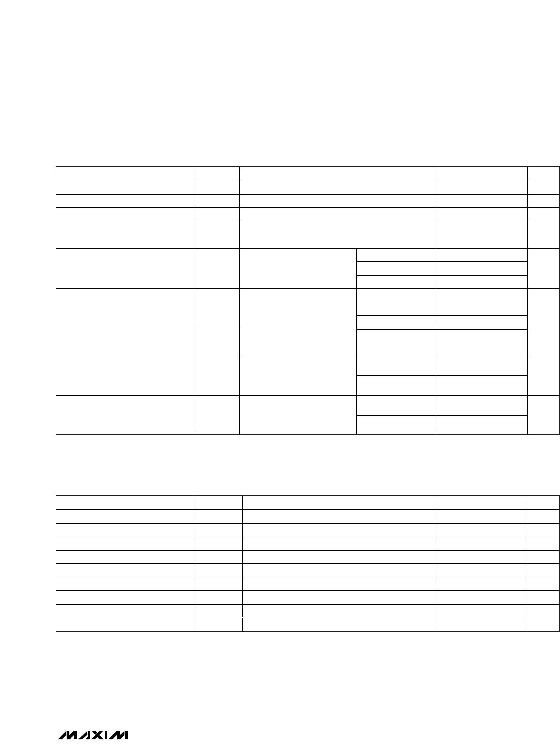
PARAMETER SYMBOL CONDITIONS MIN TYP MAX UNITS
Operating Supply Voltage V
DD
3.0 3.6 V
LEDs Anode Voltage
(R0–R7, G0–G7, B0–B7, MUX0,
and MUX1)
V
O
7V
f
CLKI
= 0Hz; CLKO_, DOUT_ loaded 200Ω;
calibration DACs set to 0x01
28 52
f
CLKI
= 0Hz; CLKO_, DOUT_ loaded 200Ω;
calibration DACs set to 0xFF
51 72
Supply Current I
DD
f
CLKI
= 32MHz; CLKO_, DOUT_ loaded 200Ω;
calibration DACs set to 0xFF
54 77
mA
Input High Voltage LOADI V
IHC
0.7
x V
DD
V
Input Low Voltage LOADI V
ILC
0.3
x V
DD
V
Differential Input Voltage Range
CLKI_, DIN_
V
ID
±0.15 ±1.20 V
Common-Mode Input Voltage
CLKI_, DIN_
V
CM
| V
I D
/ 2| 2.4 V
Differential Input High Threshold VDIFF
TH
8 100 mV
Differential Input Low Threshold VDIFF
TL
-100 -8 mV
Differential Output Voltage
CLKO_, DOUT_
V
OD
Termination 200Ω at receiver _+ and _- inputs ±190 ±550 mV
Differential Output Offset
CLKO_, DOUT_
V
OS
Termination 200Ω at receiver _+ and _- inputs 1.125 1.25 1.375 V
Input Leakage Current
CLKI_, DIN_, LOADI
I
IH
, I
IL
-1 +1 µA
Input Capacitance
CLKI_, DIN_, LOADI
10 pF
Output Low Voltage LOADO V
OLC
I
SINK
= 5mA 0.05 0.25 V
Output High Voltage LOADO V
OHC
I
SOURCE
= 5mA
V
DD
- 0.5
V
DD
- 0.2
V
ELECTRICAL CHARACTERISTICS
(V
DD
= 3.0V to 3.6V, T
A
= T
MIN
to T
MAX
, unless otherwise noted. Typical values are at V
DD
= 3.3V, T
A
= +85°C.) (Note 1)
MAX6974/MAX6975
24-Output PWM LED Drivers
for Message Boards
_______________________________________________________________________________________ 3
Note 1: All parameters tested at T
A
= +85°C. Specifications over temperature are guaranteed by design.
Note 2: Specification limits apply to devices at the same T
A
for T
A
= T
MIN
to T
MAX
.
Note 3: Guaranteed by design.
PARAMETER SYMBOL CONDITIONS MIN TYP MAX UNITS
Output Slew Time LOADO 20% to 80%, 80% to 20%, load = 10pF 3 ns
Output Low Voltage MUX_ V
OLM
I
SINK
= 40mA 0.4 V
Open-Circuit Detection V
OCD
200 mV
Output Voltage Slew Time
R0–R7, G0–G7, B0–B7
80% to 20%, load = 50pF,
calibration DACs set to 0xFF
100 ns
T
A
= +85°C 29.4 30 30.6
T
A
= +125°C 29.10 30.90
Full-Scale Port Output Current
R0–R7, G0–G7, B0–B7
I
SINKFS
V
DD
= 3.3V, V
O
= 1.2V,
calibration DACs set to 0xFF
T
A
= T
MIN
to T
MAX
28.2 31.8
mA
T
A
= +125°C
(Note 3)
0.5 1.7
T
A
= +85°C 0.3 1
Port-to-Port Current Matching
R0–R7, G0–G7, B0–B7
ΔI
SINK
V
DD
= 3.3V, V
O
= 1.2V,
calibration DACs set to 0xFF
I
SINK
= 30mA (Note 2)
T
A
= -40°C
(Note 3)
±0.9 3.0
%
T
A
= +85°C 0.3 1.15
Output Load Regulation ΔI
OLR
V
D D
= 3.3V , V
O
= 1.2V to 3.0V ,
calibration DACs set to 0x80,
I
SINK
= 18mA
T
A
= T
MIN
to T
MAX
1.5
mA/V
T
A
= +85°C 0.6 1.7
Output Power-Supply Rejection ΔI
OPSR
V
D D
= 3.0V to 3.6V , V
O
= 1.2V ,
calibration DACs set to 0x80,
I
SINK
= 18mA
T
A
= T
MIN
to T
MAX
2.0
mA/V
ELECTRICAL CHARACTERISTICS (continued)
(V
DD
= 3.0V to 3.6V, T
A
= T
MIN
to T
MAX
, unless otherwise noted. Typical values are at V
DD
= 3.3V, T
A
= +85°C.) (Note 1)
PARAMETER SYMBOL CONDITIONS MIN TYP MAX UNITS
CLKI_ Input Frequency f
CLKI
33 MHz
CLKI_ Duty Cycle 40 60 %
CLKO_ Output Delay t
PD-CLKO
19 ns
DIN_ Setup Time t
SU-DIN
0.5 ns
DIN_ Hold Time t
HD-DIN
5ns
DOUT_ Output Delay t
PD-DOUT
18 ns
LOADO Output Delay t
PD-LOADO
21 ns
LOADI Hold Time t
HD-LOADI
11 ns
Watchdog Period When enabled 40 125 300 ms
TIMING CHARACTERISTICS
(V
DD
= 3.0V to 3.6V, T
A
= T
MIN
to T
MAX
, unless otherwise noted. Typical values are at 3.3V, T
A
= +85°C.) (Note 1)

MAX6975ATL+

Mfr. #:
Manufacturer:
Maxim Integrated
Description:
LED Lighting Drivers 24-Output PWM LED Driver
Lifecycle:
New from this manufacturer.
Delivery:
DHL FedEx Ups TNT EMS
Payment:
T/T Paypal Visa MoneyGram Western Union

Products related to this Datasheet