MAX6974/MAX6975
The serial interface uses the continuously running
clock, CLKI, to synchronously transfer and latch data
(33MHz max). The MAX6974/MAX6975 sample inputs
DIN and LOADI on the rising edge of CLKI and update
outputs DOUT and LOADO on the rising edge of CLKI.
The MAX6974/MAX6975 specifications guarantee that
cascaded devices observe setup and hold timing from
device to device, making external buffers and clock
trees unnecessary, even in very large systems.
The high-speed CLKI, CLKO, DIN, and DOUT signals
use low-voltage differential signaling (LVDS), and the
less frequently changing control signals, LOADI and
LOADO, use standard CMOS. The differential signals
are generally referred to in unipolar shorthand; for
example, the statement “CLKI rising edge” means that
CLKI+ is rising, and CLKI- is falling.
The MAX6974/MAX6975 use LVDS drivers with differential
signaling (300mV nominal logic swing around a +1.2V
bias) and cascaded CMOS control signals to minimize
signal-path EMI and simplify interface timing and print-
ed-circuit board (PCB) layout. Note the differential
inputs for the first driver can be driven from +3.3V
CMOS using LVDS level translators, such as the
MAX9112 terminated with 110Ω (see Figure 12).
A 25MHz to 33MHz clock frequency is recommended
to keep the display refresh rate high. When using the
MAX6975 in reduced global-intensity mode (GLB4 = 1
in configuration register), the recommended clock
frequency range is 6MHz to 33MHz.
Serial-Interface Protocol Structure
The MAX6974/MAX6975 serial interface transfers all
data and control functions using a protocol structure
consisting of header, data, and optional tail segments
transmitted in this sequence. The header and tail
24-Output PWM LED Drivers
for Message Boards
16 ______________________________________________________________________________________
t
HD-DIN
t
HD-LOADI
CLKI+
CLKI-
CLKO+
CLKO-
DIN+
DIN-
DOUT+
DOUT-
LOADI
LOADO
t
PD-CLKO
t
SU-DIN
t
PD-DOUT
t
PD-LOADO
t
SU-LOADI
Figure 6. Serial-Interface Timing
segments transfer to all cascaded devices, while the
data section reduces in bit length as data transfers
through the cascaded devices. When LOADI is low, the
MAX6974/MAX6975 continuously monitor DIN for
reception of the SYNC pattern (see the
Header
Segment
section).
Header Segment
The 24-bit header segment consists of an 8-bit fixed
synchronization pattern (SYNC), a 6-bit command pat-
tern (CMD), and a 10-bit counter (CNTR) segment (see
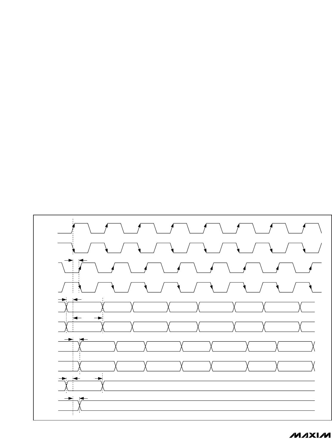
Table 7). LOADI must change from low to high within
plus or minus one clock cycle of the first command bit.
When the SYNC bit pattern 0xE8 is recognized, LOADI
is monitored for the rising edge, allowing the device to
internally synchronize LOADI to CLKI. The six command
bits, CMD[5:0], consist of bits C1 and C0 repeated
three times. The four commands used by the MAX6974/
MAX6975 are defined by the two bits, C1 and C0.
The counter segment is incremented by one for each
cascaded device with an internal fault detected. Use the
counter segment to collect fault data across the cas-
caded chain.
HDR[23:0]
Complete 24-bit header segment.
SYNC[7:0]
Synchronization bit pattern 0xE8 is recognized by the
MAX6974/MAX6975 during intervals when LOADI is low.
The SYNC bit pattern, followed by the rising edge of
LOADI, internally synchronizes the timing relationship
between CLKI and DIN with the LOADI signal. The
synchronization pattern must be 0xE8.
CMD[5:0]
Send command bits C1 and C0 three times in succes-
sion. The command bits define how many data bits are
received and where the data is loaded. The four com-
mands are:
CNTR[9:0]
This is the counter for open LED or overtemperature fault
conditions. The host sends the header segment with the
counter value set to zero. The counter value is incre-
mented one count by each device that detects a fault
condition in the cascaded chain. The accumulated count
value returns to the host from the last device in the cas-
cade chain. The command determines which fault type
is incremented to the counter (see
LED Open-Circuit and
Overtemperature Detection Counter
section):
CMD[1:0] = X0 Overtemperature faults counted
CMD[1:0] = X1 Open LED faults counted
MAX6974/MAX6975
24-Output PWM LED Drivers
for Message Boards
______________________________________________________________________________________ 17
HDR
23 22 21 20 19 18 17 16 15 14 13 12 11 10 9 8 7 6 5 4 3 2 1 0
SYNC CMD CNTR
765432101010109876543210
1 1 1 0 1 0 0 0 C1C0C1C0C1C0b9b8b7b6b5b4b3b2b1b0
Table 7. Serial-Interface Header
C1:C0 COMMAND CMD[5:0]
00 Load individual PWM 000000
01 Load CALDAC 010101
10 Load global-intensity PDM 101010
11 Load configuration 111111
HEADER
COUNTER
CLKI
COMMAND
11101000
SYNC
LOADI
1
2
3
4
5
6
7
8
9
10
11
12
13
14
15
16
17
18
19
20
21
22
23
24
25
26
27
28
DIN
1
0
(CONTINUOUS)
C1 C0 C1 C0 C1 C0
b9 b8 b7 b6 b5 b4 b3 b2
DATA
b1 b0
Figure 7. Header-Segment Timing
MAX6974/MAX6975
Data Segment
The bit length of the data segment received by the
MAX6974/MAX6975 is dependent on the command
specified in the header.
The load CALDAC command has three unique data
bytes, while load global-intensity PDM and load
configuration each have one byte of data repeated
three times. The CALDAC data within the command
load CALDAC is sent with B CALDAC data first, fol-
lowed by G CALDAC data, and then R CALDAC data,
as shown in Table 8.
The data segment of the load individual PWM command
has a variable length depending on specific device and
configuration settings. The data is always organized
as B driver data first in the order of B7 first to B0 last
(MSB first), followed by the G driver data in the same
order of G7 to G0 (MSB first), and then the R driver data
in the order of R7 to R0 (MSB first).
Tail Segment
The MAX6974/MAX6975 allow for an optional string of
data bits to be transmitted following all device data
bits, which is referred to as the tail segment. The data
bits of the tail segment are clocked back to the host,
following the header, from the last device in a cascaded
chain. The number of bits in the tail segment is optional.
The tail carries no device-specific data on DIN, but
provides feedback confirmation to the host that all data
bits were extracted by all devices in the cascade chain.
24-Output PWM LED Drivers
for Message Boards
18 ______________________________________________________________________________________
HEADER DATA 1 DATA 2 DATA 3 DATA N
HDR[23:0] B[7:0] G[7:0] R[7:0] B[7:0] G[7:0] R[7:0] B[7:0] G[7:0] R[7:0] B[7:0] G[7:0] R[7:0]
Table 8. Serial Format for Load CALDAC
HEADER DATA 1 DATA 2 DATA 3 DATA N
HDR[23:0] D[7:0] D[7:0] D[7:0] D[7:0] D[7:0] D[7:0] D[7:0] D[7:0] D[7:0] D[7:0] D[7:0] D[7:0]
Table 9. Serial Format for Load Global-Intensity PDM
HEADER DATA 1 DATA 2 DATA 3 DATA N
HDR[23:0] D[7:0] D[7:0] D[7:0] D[7:0] D[7:0] D[7:0] D[7:0] D[7:0] D[7:0] D[7:0] D[7:0] D[7:0]
Table 10. Serial Format for Load Configuration
HEADER DATA 1 DATA 2 DATA 3 DATA N
HDR[23:0] B7, B6, …R0 B7, B6, …R0 B7, B6, …R0 B7…R0
Table 11. Serial Format for Load Individual PWM (Nonmultiplexed)
HEADER DATA 1 DATA 2 DATA 3 DATA N
HDR[23:0] B7, B7', B6, B6', …R0' B7, B7', B6, B6', …R0' B7, B7', B6, B6', …R0' B7, B7', B6, B6', …R0'
Table 12. Serial Format for Load Individual PWM (Multiplexed)
B[7:0] 8-bit data loaded into port B CALDAC
G[7:0] 8-bit data loaded into port G CALDAC
R[7:0] 8-bit data loaded into port R CALDAC
N Number of cascaded devices
D[7:0] Send the 8-bit data for the global-intensity PDM three times (24 total bits)
D[7:0] Send the 8-bit configuration data three times (24 total bits)
B_…G_…R_ 12-bit (MAX6974) or 14-bit (MAX6975) data each
B_ 12-bit (MAX6974) or 14-bit (MAX6975) PWM data for each output B_ during multiplex phase MUX0, MSB first
B_' 12-bit (MAX6974) or 14-bit (MAX6975) PWM data for each output B_ during multiplex phase MUX1, MSB first
G_ 12-bit (MAX6974) or 14-bit (MAX6975) PWM data for each output G_ during multiplex phase MUX0, MSB first
G_' 12-bit (MAX6974) or 14-bit (MAX6975) PWM data for each output G_ during multiplex phase MUX1, MSB first
R_ 12-bit (MAX6974) or 14-bit (MAX6975) PWM data for each output R_ during multiplex phase MUX0, MSB first
R_' 12-bit (MAX6974) or 14-bit (MAX6975) PWM data for each output R_ during multiplex phase MUX1, MSB first

MAX6975ATL+

Mfr. #:
Manufacturer:
Maxim Integrated
Description:
LED Lighting Drivers 24-Output PWM LED Driver
Lifecycle:
New from this manufacturer.
Delivery:
DHL FedEx Ups TNT EMS
Payment:
T/T Paypal Visa MoneyGram Western Union

Products related to this Datasheet