Serial-Interface Cascade Timing
The MAX6974/MAX6975 serial-interface protocol timing
is simplified by the guaranteed setup and hold charac-
teristics of the outputs from one device driving the
inputs of another. An example of a cascade of three
MAX6974/MAX6975 devices is shown in Figure 8.
Example of Serial-Interface
Cascade Timing
The basic timing of a MAX6974/MAX6975 cascaded
chain of three devices demonstrates the principle that
applies to any number of cascaded devices. The first
device connected to the host transmitter is referenced
as 1, and the remaining devices are referenced as 2
and 3. Device 3 outputs connect to the host for commu-
nicating diagnostic and fault counter data.
The first MAX6974/MAX6975, device 1, receives the
header and captures the first set of data bits. The
number of captured bits is determined by the command
given in the header. A timing example of the data trans-
fer for the Load CALDAC command is shown in Figure
9. Device 1 does not send the captured data out on
DOUT. Instead, device 1 sends out a new header 25
clock cycles after the reception of the first header bit on
DIN. The data flow on each interconnect node is shown
in Figure 10.
After capturing the first data set, device 1 transmits all
following data segments and the optional tail segment
on DOUT, delayed by one CLKI cycle. Device 2
receives the new header from device 1, followed by
data that now begins with device 2’s data set. Device 2
repeats the same process as described above; captur-
ing the first data set received, appending a new head-
er, and passing all subsequent data out DOUT to the
next device 3. Device 3 captures the last data set and
transmits a header followed by the tail segment. The
last header and tail segments are clocked back into the
host receiver. The header received by the host contains
the updated fault counter data. The tail data bit pattern
can be compared to the tail data originally transmitted
by the host for data integrity check.
MAX6974/MAX6975
24-Output PWM LED Drivers
for Message Boards
______________________________________________________________________________________ 19
HOST
CLKO
DOUT
LOADO
CLKI
DIN
LOADI
CLK0
D0
LOAD0
CLK1
D1
LOAD1
CLK2
D2
LOAD2
CLK3
D3
LOAD3
MAX6974/MAX6975
1
MAX6974/MAX6975
2
MAX6974/MAX6975
3
CLKI
DIN
LOADI
CLKO
DOUT
LOADO
CLKI
DIN
LOADI
CLKO
DOUT
LOADO
CLKI
DIN
LOADI
CLKO
DOUT
LOADO
Figure 8. Example Showing Three-Device Cascade Connection Scheme with the Interconnecting Nodes Labeled for Clarity
DATA: CALDAC DATA 1
(CONTINUOUS)
25
26
27
28
29
30
31
32
33
34
35
36
37
38
39
40
41
42
43
44
45
46
47
48
49
50
51
52
53
54
55
56
57
58
59
60
61
62
63
64
65
66
67
68
69
70
71
72
CLKI
LOADI
DIN
0
1
B CALDAC G CALDAC G CALDAC B CALDAC G CALDAC R CALDAC
DATA: CALDAC DATA 2
D7 D6 D5 D4 D3 D2 D1 D0
D7 D6 D5 D4 D3 D2 D1 D0 D7 D6 D5 D4 D3 D2 D1 D0 D7 D6 D5 D4 D3 D2 D1 D0 D7 D6 D5 D4 D3 D2 D1 D0 D7 D6 D5 D4 D3 D2 D1 D0
Figure 9. Timing Example Showing CALDAC Data Set for the First Two Cascaded Devices
IDLE
IDLE
IDLE
IDLE
CLK0
3 BYTES 1 3 BYTES 2 3 BYTES 3HEADER 1
T
3 BYTES 2 3 BYTES 3HEADER 2 T
3 BYTES 3HEADER 3
T
HEADER 4
T
25 CLOCKS
25 CLOCKS
25 CLOCKS
D0
D1
D2
D3
Figure 10. Data Cascading Example for 24-Bit Data Words
MAX6974/MAX6975
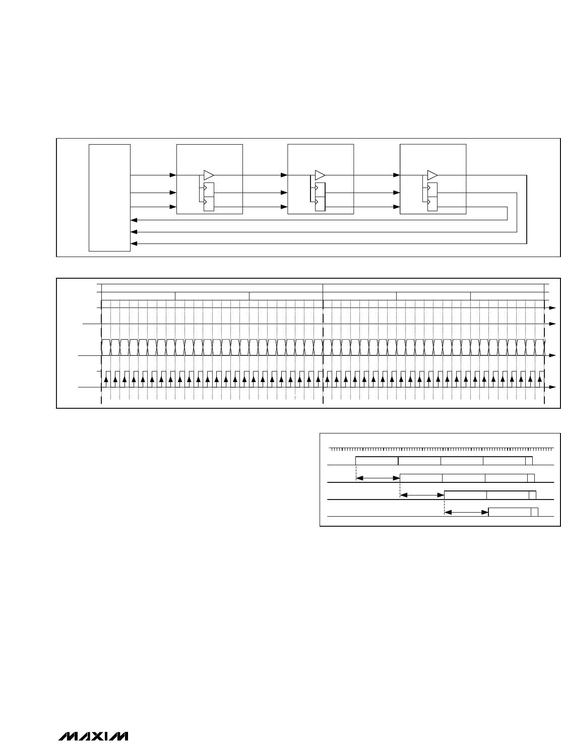
When the MAX6974/MAX6975 send individual-intensity
PWM data, the data segment bit length is large due to
the 12-bit or 14-bit PWM data for each of the 24 outputs
(see Figure 11). The various data segment bit lengths
for each of the four commands and different operating
modes is shown in Table 4. Data capturing is the same
as described above with the header segment outputs
and data being delayed by the full length of the data bit
stream being captured plus one clock cycle.
LED Open-Circuit and
Overtemperature Detection Counter
The MAX6974/MAX6975 feature LED open-circuit
detection and overtemperature detection that use the
counter section of the header segment to record
detected faults. Using commands 01 or 11 force the
counter to record LED open-circuit detection faults.
Using commands 00 or 10 force the counter to record
overtemperature faults.
The MAX6974/MAX6975 detect an open circuit on a driver
output by monitoring for output voltages below 200mV.
When an open circuit is detected, the MAX6974/
MAX6975 increment the counter segment data,
CNTR[9:0], received on DIN by 1 before transmitting a
header and new counter value out DOUT. Regardless
of the number of open-circuit outputs on a device, the
counter increment is 1.
The MAX6974/MAX6975 detect die temperatures above
T
DIE
= +165°C and disable all output drivers by setting
all PWM data to zero. During an overtemperature event,
the MAX6974/MAX6975 increment the counter segment
data, CNTR[9:0], received on DIN by 1 before transmitting
a header and new counter value out DOUT. The output
drivers are allowed to be on when the die temperature
falls below T
DIE
= +150°C.
When there is no fault detected, the counter data is
passed directly to DOUT unaltered.
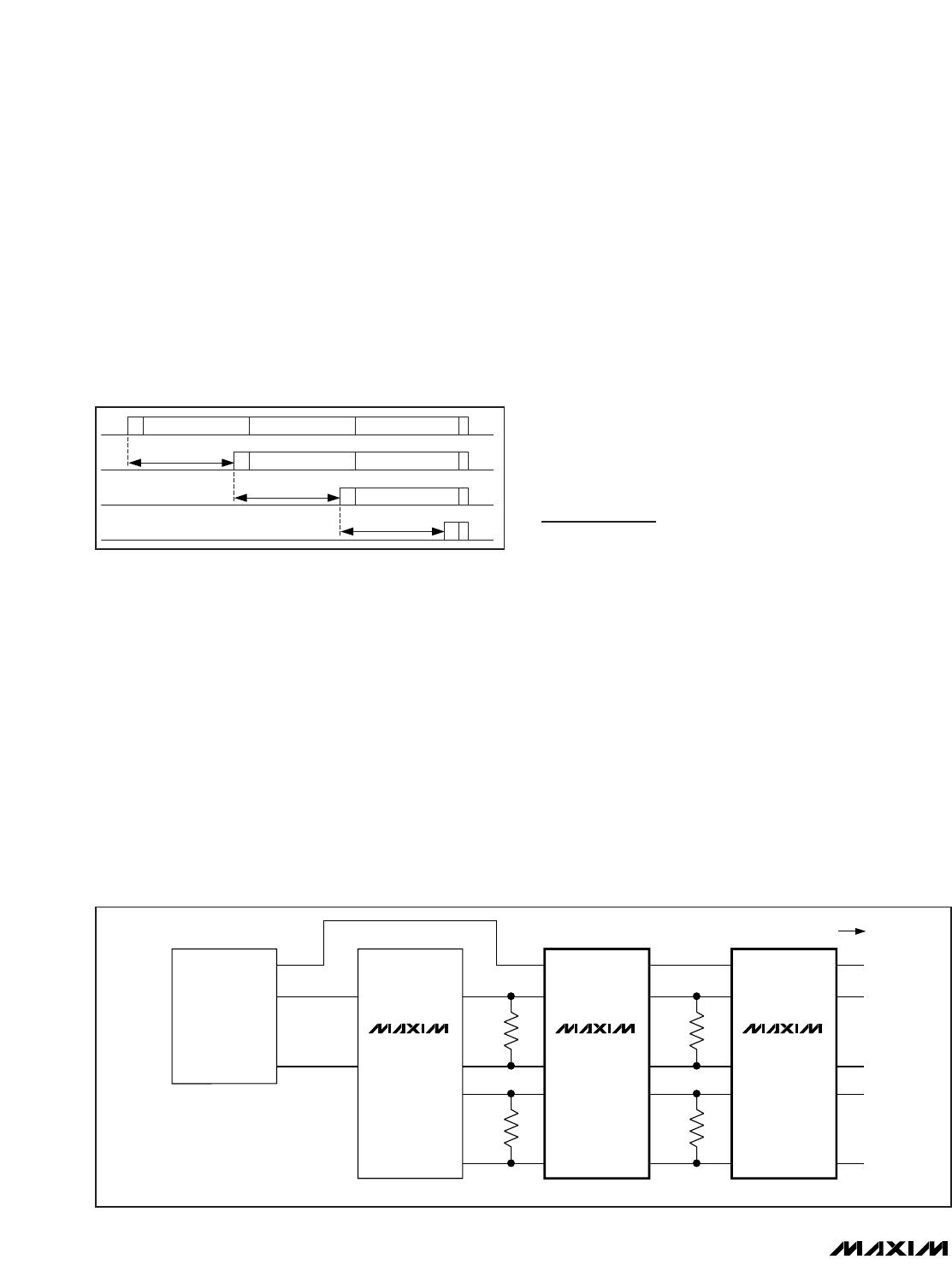
Applications Information
Terminations and PCB Layout
The MAX6974/MAX6975’s layout simplifies cascading
multiple devices, as the interface signals flow through
from each device. The synchronous and buffered
nature of the interface simplifies the board design, but
pay attention to signal routing and termination, as with
other high-speed logic circuits.
Terminate the differential input pairs, CLKI+ and CLKI-,
as well as DIN+ and DIN-, with a termination resistor as
close as possible to the package. When using the
MAX6974/MAX6975 as the signal source, use a 200Ω
termination resistor. When using a level translator or clock
retimer as the signal source, use a 110Ω termination
resistor. Route each differential input pair as close
parallel tracks with spacing or a GND trace between
the track pair and the next signal track to minimize
cross-coupling. Track lengths up to a few inches do not
require termination-matched tracks (transmission lines).
24-Output PWM LED Drivers
for Message Boards
20 ______________________________________________________________________________________
DATA 1 PWM 288 BITSH1
289 CLOCKS
289 CLOCKS
289 CLOCKS
D0
D1
D2
D3
DATA 2 PWM 288 BITS DATA 3 PWM 288 BITS
T
DATA 2 PWM 288 BITS DATA 3 PWM 288 BITS
T
H2
DATA 3 PWM 288 BITS
T
H3
T
H4
Figure 11. Long (288 Bits) PWM Data Cascading Shown for
MAX6974 in Nonmultiplexed Mode
CLKI- CLKO-
CLKO+
CLKI+
200Ω
DIN- DOUT-
DOUT+
DIN+
LOADO
LOADI
n-2
200Ω
MAX6974
CLKI- CLKO-
CLKO+
CLKI+
110Ω
DIN- DOUT-
DOUT+
DIN+
LOADO
LOADI
n-1
110Ω
MAX6974
DO2-
DO2+
DIN2 DO1-
DO1+
DIN1
MAX9112
CLK
DIN
LOAD
HOST
n MORE DEVICES WITH
200Ω TERMINATION
Figure 12. Typical Cascaded Serial-Interface Termination Circuit
MAX6974/MAX6975
24-Output PWM LED Drivers
for Message Boards
______________________________________________________________________________________ 21
Use the same length interface signal paths, whether
differential or CMOS, to ensure a uniform propagation
delay for each signal.
Power-Supply Considerations
The MAX6974/MAX6975 operate with a power-supply
voltage of 3.0V to 3.6V. Bypass the V
DD
power supply
to GND with a 0.1µF ceramic capacitor as close as
possible to the device pins. If the LED supply is shared
with the V
DD
supply, adequately decouple the V
DD
supply with bulk capacitance to ensure that the fast-
rising, high-current LED drive currents do not cause
transient dips in V
DD
.
Driving LEDs from a Supply Higher than 7V
An external npn transistor in a cascode configuration
extends the output drive voltage above 7V. The external
pass transistor’s emitter clamps to a V
BE
below its
base, which is connected to the MAX6974/MAX6975’s
supply voltage. An optional emitter resistor reduces the
voltage drop across the MAX6974/MAX6975’s output
transistor and effectively takes the dissipation off the
device into the resistor. The external transistor’s collector
current is equal to its emitter current (less a small base
current), and the MAX6974/MAX6975 accurately
control the emitter current with a constant current sink
driver structure.
Example of using an external npn transistor:
V
DD
= 3.3V ±5%, I
OUT
= 30mA, external pass transistor
V
BE
= 0.7V to 1V at 30mA emitter current.
For best output current accuracy, design V
O
to be at
least 1.2V:
R1
(MAX)
= (3.15 - 1 - 1.2) / 0.030 = 31.7Ω, so choose
R1 = 30Ω.
MAX6974
MAX6975
V
DD
R1
Q1
30mA
+3.3V +3.3V +24V
R1
R2
R3
R4
R5
R6
R7
R0
GND
Figure 13. External Cascode npn Transistor
MAX6974 MAX6974
SYSTEM
CLK
DATA
LOAD
CLKO
DINO
LOADO
CLKI
DINI
LOADI
R0/G0/B0
8 RGB LEDs
R1/G1/B1
R2/G2/B2
R3/G3/B3
R4/G4/B4
R5/G5/B5
R6/G6/B6
R7/G7/B7
R0/G0/B0
R1/G1/B1
R2/G2/B2
R3/G3/B3
R4/G4/B4
R5/G5/B5
R6/G6/B6
R7/G7/B7
CLKO
DINO
LOADO
CLKI
DINI
LOADI
Typical Operating Circuit
Chip Information
PROCESS: BiCMOS

MAX6975ATL+

Mfr. #:
Manufacturer:
Maxim Integrated
Description:
LED Lighting Drivers 24-Output PWM LED Driver
Lifecycle:
New from this manufacturer.
Delivery:
DHL FedEx Ups TNT EMS
Payment:
T/T Paypal Visa MoneyGram Western Union

Products related to this Datasheet