LTC4070
1
4070fc
Typical applicaTion
DescripTion
Li-Ion/Polymer Shunt
Battery Charger System
The LTC
®
4070 allows simple charging of Li-Ion/Polymer
batteries from very low current, intermittent or continuous
charging sources. The 450nA to 50mA operating cur-
rent makes charging possible from previously unusable
sources. With the addition of an external pass device,
shunt current may be boosted to 500mA. Stacked cell high
voltage battery packs are inherently balanced with shunt
charging. With its low operating current, the LTC4070 is
well suited to charge thin film batteries in energy harvesting
applications where charging sources may be intermittent
or very low power. The unique architecture of the LTC4070
allows for an extremely simple battery charger solution;
requiring just one external resistor.
The LTC4070 offers a pin selectable float voltage with 1%
accuracy across the full range of operating temperature
and shunt current. The integrated thermal battery quali-
fier extends battery lifetime and improves reliability by
automatically reducing the battery float voltage at NTC
thermistor temperatures above 40°C. The LTC4070 also
provides both low and high battery status outputs. For
applications requiring pack protection, see LTC4071.
The device is offered in two thermally enhanced packages,
a compact low profile (0.75mm) 8-lead (2mm × 3mm)
DFN and an 8-lead MSOP package.
FeaTures
applicaTions
n
Low Operating Current (450nA)
n
1% Float Voltage Accuracy Over Full Temperature
and Shunt Current Range
n
50mA Maximum Internal Shunt Current
(500mA with External PFET)
n
Pin Selectable Float Voltage Options:
4.0V, 4.1V, 4.2V
n
Ultralow Power Pulsed NTC Float Conditioning for
Li-Ion/Polymer Protection
n
Suitable for Intermittent, Continuous and Very Low
Power Charging Sources
n
Low and High Battery Status Outputs
n
Simple Low Voltage Load Disconnect Application
n
Thermally Enhanced, Low Profile (0.75mm)
8-Lead (2mm × 3mm) DFN and MSOP Packages
n
Low Power Li-Ion/Polymer Battery Back-Up
n
Solar Power Systems with Back-Up
n
Memory Back-Up
n
Embedded Automotive
n
Thin Film Batteries
n
Energy Scavenging/Harvesting
L, LT, LTC, LTM, Linear Technology and the Linear logo are registered trademarks and
ThinSOT is a trademark of Linear Technology Corporation. All other trademarks are the property
of their respective owners..
NTC Overtemperature Battery Float
Voltage Qualifying
Simple Shunt Charger with Load Disconnect
and NTC Conditioning
TEMPERATURE (°C)
V
F
(V)
4.3
4.2
4.0
4.1
3.9
3.8
3.7
4020
0
60
4070 TA01b
80 100
ADJ = V
CC
ADJ = FLOAT
ADJ = GND
4070 TA01a
LTC4070
ADJ
R
IN
GND
T
10k
Li-Ion
NTCBIAS
LBO
NTC
V
CC
V
IN
+
NTHS0805N02N1002F
Q1:FDR8508
LTC4070
2
4070fc
absoluTe MaxiMuM raTings
I
CC
....................................................................... ±60mA
ADJ, NTC, NTCBIAS, DRV, LBO, HBO
Voltages ...........................................0.3V to V
CC
+ 0.3V
Operating Junction Temperature Range .. 40°C to 125°C
(Notes 1, 2)
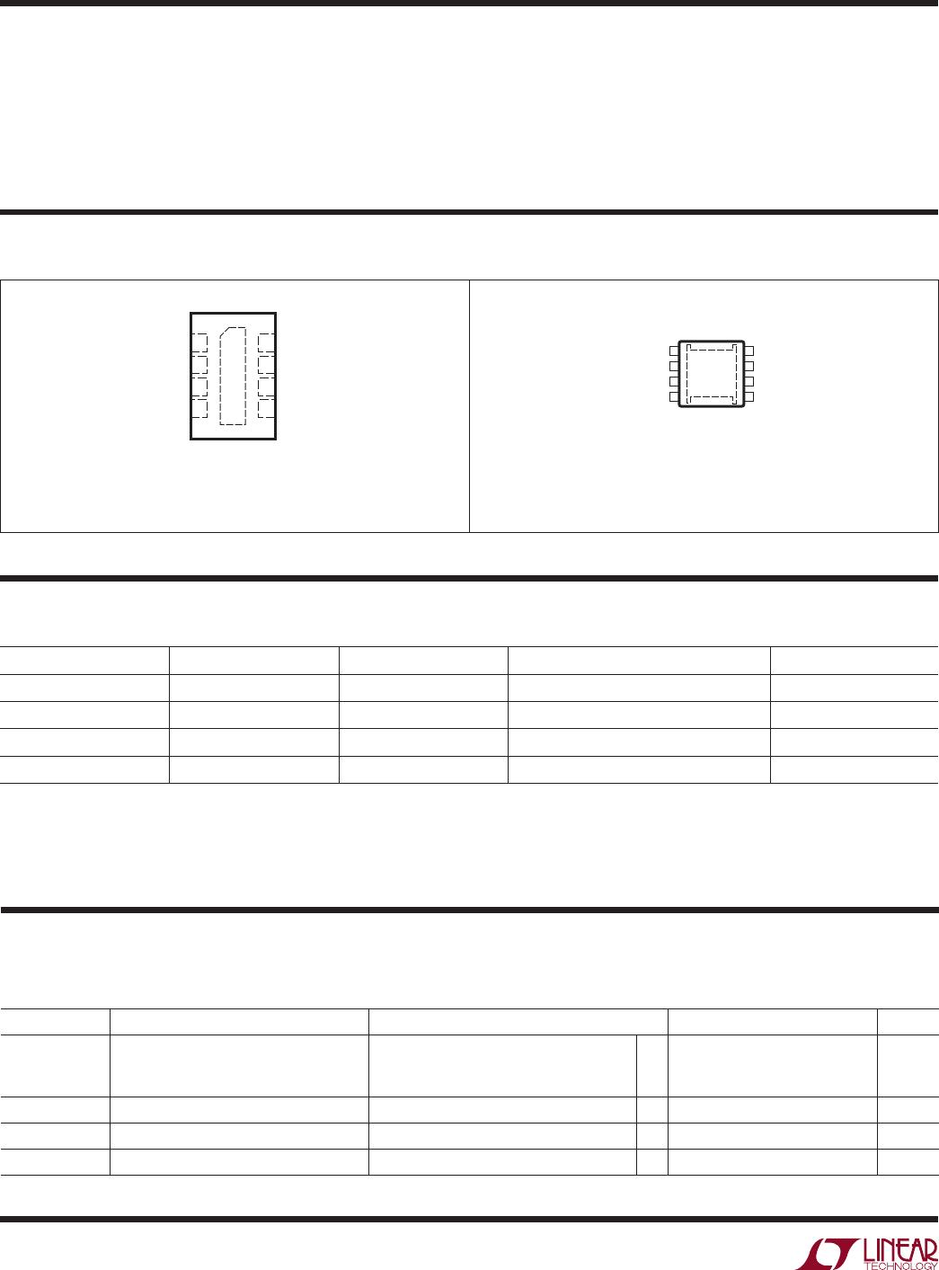
TOP VIEW
9
DDB PACKAGE
8-LEAD (3mm × 2mm) PLASTIC DFN
5
6
7
8
4
3
2
1NTCBIAS
NTC
ADJ
HBO
V
CC
DRV
LBO
GND
T
JMAX
= 125°C, q
JA
= 76°C/W
EXPOSED PAD (PIN 9) IS NOT INTERNALLY CONNECTED,
MUST BE SOLDERED TO PCB, GND TO OBTAIN q
JA
1
2
3
4
NTCBIAS
NTC
ADJ
HBO
8
7
6
5
V
CC
DRV
LBO
GND
TOP VIEW
9
MS8E PACKAGE
8-LEAD PLASTIC MSOP
T
JMAX
= 125°C, q
JA
= 40°C/W
EXPOSED PAD (PIN 9) IS NOT INTERNALLY CONNECTED,
MUST BE SOLDERED TO PCB, GND TO OBTAIN q
JA
pin conFiguraTion
orDer inForMaTion
LEAD FREE FINISH TAPE AND REEL PART MARKING* PACKAGE DESCRIPTION TEMPERATURE RANGE
LTC4070EDDB#PBF LTC4070EDDB#TRPBF LFPD 8-Lead (3mm × 2mm) Plastic DFN –40°C to 125°C
LTC4070IDDB#PBF LTC4070IDDB#TRPBF LFPD 8-Lead (3mm × 2mm) Plastic DFN –40°C to 125°C
LTC4070EMS8E#PBF LTC4070EMS8E#TRPBF LTFMT 8-Lead Plastic MSOP –40°C to 125°C
LTC4070IMS8E#PBF LTC4070IMS8E#TRPBF LTFMT 8-Lead Plastic MSOP –40°C to 125°C
Consult LTC Marketing for parts specified with wider operating temperature ranges. *The temperature grade is identified by a label on the shipping container.
Consult LTC Marketing for information on non-standard lead based finish parts.
For more information on lead free part marking, go to: http://www.linear.com/leadfree/
For more information on tape and reel specifications, go to: http://www.linear.com/tapeandreel/
Maximum Junction Temperature ......................... 125°C
Storage Temperature Range .................. 65°C to 150°C
Peak Reflow Temperature ..................................... 260°C
SYMBOL PARAMETER CONDITIONS MIN TYP MAX UNITS
V
FLOAT
Programmable Float Voltage
10µA ≤ I
CC
≤ 50mA
V
ADJ
= 0V
V
ADJ
= Float
V
ADJ
= V
CC
l
l
l
3.96
4.06
4.16
4.0
4.1
4.2
4.04
4.14
4.24
V
V
V
I
CCMAX
Maximum Shunt Current V
CC
> V
FLOAT
l
50 mA
I
CCQ
V
CC
Operating Current V
HBO
Low
l
450 1040 nA
I
CCQLB
Low Bat V
CC
Operating Current V
CC
= 3.1V 300 nA
elecTrical characTerisTics
The l denotes the specifications which apply over the full operating
junction temperature range. V
NTC
= V
CC
, T
A
= 25°C unless otherwise specified. Current into a pin is positive and current out of a pin is
negative. All voltages are referenced to GND unless otherwise noted. (Note 2)
LTC4070
3
4070fc
elecTrical characTerisTics
Note 1: Stresses beyond those listed under Absolute Maximum Ratings
may cause permanent damage to the device. Exposure to any Absolute
Maximum Rating condition for extended periods may affect device
reliability and lifetime.
Note 2: The LTC4070 is tested under pulsed load conditions such that
T
J
≈ T
A
. The LTC4070E is guaranteed to meet performance specifications
for junction temperatures from 0°C to 85°C. Specifications over the
–40°C to 125°C operating junction temperature range are assured by
design, characterization and correlation with statistical process controls.
The l denotes the specifications which apply over the full operating
junction temperature range. V
NTC
= V
CC
, T
A
= 25°C unless otherwise specified. Current into a pin is positive and current out of a pin is
negative. All voltages are referenced to GND unless otherwise noted. (Note 2)
The LTC4070I is guaranteed over the full –40°C to 125°C operating
junction temperature range. Note that the maximum ambient temperature
consistent with these specifications is determined by specific operating
conditions in conjunction with board layout, the rated package thermal
resistance and other environmental factors.
Note 3: The I
DRV(SNK)
current is tested by pulling the DRV pin up to V
CC
through a 475k resistor, R
DRV
. Pulling the DRV pin up to V
CC
with low
impedance disables the regulator.
SYMBOL PARAMETER CONDITIONS MIN TYP MAX UNITS
High Battery Status
V
HBTH
HBO Threshold (V
FLOAT
– V
CC
) V
CC
Rising
l
15 40 60 mV
V
HBHY
Hysteresis 100 mV
Low Battery Status
V
LBTH
LBO Threshold V
CC
Falling
l
3.08 3.2 3.34 V
V
LBHY
Hysteresis 220 290 350 mV
Status Outputs HBO/LBO
V
OL
CMOS Output Low I
SINK
= 1mA, V
CC
= 3.7V
l
0.5 V
V
OH
CMOS Output High V
LBO
: V
CC
= 3.1V, I
SOURCE
= –100µA
V
HBO
: I
CC
= 1.5mA, I
SOURCE
= –500µA
l
V
CC
– 0.6 V
3-State Selection Input: ADJ
V
ADJ
ADJ Input Level Input Logic Low Level
l
0.3 V
Input Logic High Level
l
V
CC
– 0.3 V
I
ADJ(Z)
Allowable ADJ Leakage Current in
Floating State
l
±3 µA
NTC
I
NTC
NTC Leakage Current 0V< NTC < V
CC
–50 0 50 nA
I
NTCBIAS
Average NTCBIAS Sink Current Pulsed Duty Cycle < 0.002% 30 pA
∆V
FLOAT(NTC)
Delta Float Voltage per NTC Comparator
Step
I
CC
= 1mA, NTC Falling Below One of the
NTC
TH
Thresholds
ADJ = 0V
ADJ = Float
ADJ = V
CC
–50
–75
–100
mV
mV
mV
NTC
TH1
NTC Comparator Falling Thresholds V
NTC
as % of V
NTCBIAS
Amplitude 35.5 36.5 37.5 %
NTC
TH2
28.0 29.0 30.0 %
NTC
TH3
21.8 22.8 23.8 %
NTC
TH4
16.8 17.8 18.8 %
NTC
HY
Hysteresis 30 mV
Drive Output
I
DRV(SOURCE)
DRV Output Source Current V
CC
= 3.1V, V
DRV
= 0V –1 mA
I
DRV(SINK)
DRV Output Sink Current I
CC
= 1mA, R
DRV
= 475k (Note 3) 3 µA

LTC4070EDDB#TRMPBF

Mfr. #:
Manufacturer:
Analog Devices / Linear Technology
Description:
Battery Management Simple Low-IQ Battery Charger/Protector with NTC Thermistor Input
Lifecycle:
New from this manufacturer.
Delivery:
DHL FedEx Ups TNT EMS
Payment:
T/T Paypal Visa MoneyGram Western Union