LTC4070
10
4070fc
applicaTions inForMaTion
The voltage at the NTC pin depends on the ratio of the NTC
thermistor value, R
NTC
, and a bias resistor, R
NOM
. Choose
R
NOM
equal to the value of the thermistor at 25°C. R
NOM
is 10k for a Vishay NTHS0402N02N1002F thermistor with
a B
25/85
value of 3490. R
NOM
must be connected from
NTCBIAS to NTC. The ratio of the NTC pin voltage to the
NTCBIAS voltage is:
NTC
R
NTC
+ R
NOM
( )
When the thermistor temperature rises, the resistance
drops; and the resistor divider between R
NOM
and the
thermistor lowers the voltage at the NTC pin.
An NTC thermistor with higher B
25/85
values may also
be used with the LTC4070. However the temperature trip
points are shifted due to the higher negative temperature
coefficient of the thermistor. To correct for this difference
add a resistor, R
FIX
, in series with the higher B
25/85
value
thermistor to shift the ratio,
R
FIX
+
R
NTC
R
FIX
+ R
NTC
+ R
NOM
( )
up to the internal resistive divider tap points: NTC
TH1
through NTC
TH4
. For a 100k thermistor with a B
25/85
value
of 3950 NTHS0402N01N1003F, at 70°C (with R
NOM
=
100k) choose R
FIX
= 3.92kΩ. The temperature trip points
are found by looking up the thermistor R/T values plus
R
FIX
that correspond to the ratios for NTC
TH1
= 36.5%,
NTC
TH2
= 29.0%, NTC
TH3
= 22.8%, and NTC
TH4
= 17.8%.
Selecting R
FIX
= 3.92k results in trip points of 39.9°C,
49.4°C, 59.2°C and 69.6°C.
Another technique may be used without adding an
additional component. Instead decrease R
NOM
to adjust
the NTC
TH
thresholds for a given R/T thermistor profile. For
example, if R
NOM
= 88.7k (with the same 100k thermistor)
then the temperature trip points are 41.0°C, 49.8°C, 58.5°C,
and 67.3°C.
When using the NTC features of the LTC4070 it is important
to keep in mind that the maximum shunt current increases
as the float voltage, V
FLOAT_EFF
drops with NTC conditioning.
Reviewing the Typical Application with a 12V wall adapter
in Figure 1; the input resistor, R
IN
, should be increased
to 165Ω such that the maximum shunt current does not
exceed 50mA at the lowest possible float voltage due to
NTC conditioning, V
FLOAT_MIN
= 3.8V.
Thermal Considerations
At maximum shunt current, the LTC4070 may dissipate up
to 205mW. The thermal dissipation of the package should
be taken into account when operating at maximum shunt
current so as not to exceed the absolute maximum junc-
tion temperature of the device. With q
JA
of 40°C/W, in the
MSOP package, at maximum shunt current of 50mA the
junction temperature rise is about 8°C above ambient.
With q
JA
of 76°C/W in the DFN package, at maximum
shunt current of 50mA the junction temperature rise is
about 16°C above ambient.
Operation with an External PFET to Boost Shunt Current
Table 2 lists recommended devices to increase the
maximum shunt current. Due to the requirement for low
capacitance on the DRV pin node, it is recommended that
only low gate charge and high threshold PFET devices be
used. Also it is recommended that careful PCB layout be
used to keep leakage at the DRV pin to a minimum as the
I
DRV(SINK)
current is typically 3µA.
Refer to device manufacturers data sheets for maximum
continuous power dissipation and thermal resistance when
selecting an external PFET for a particular application.
Table 2. Recommended External Shunt PFETS
DEVICE VENDOR Q
GS
V
TH(MIN)
R
DS(ON)
FDN352AP Fairchild 0.50nC –0.8V 0.33
Si3467DV Vishay 1.7nC –1.0V 0.073
Si3469DV Vishay 3.8nC –1.0V 0.041
DMP2130LDM Diodes Inc. 2.0nC –0.6V 0.094
DMP3015LSS Diodes Inc. 7.2nC –1.0V 0.014
LTC4070
11
4070fc
Typical applicaTions
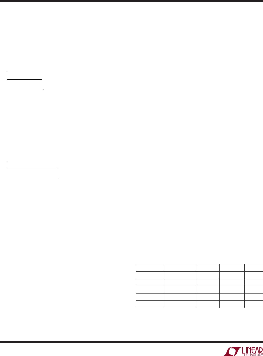
The LTC4070 can be used to charge a battery to a 4.2V
float voltage from an AC line with a bridge rectifier as
shown in the simple schematic in Figure 5. In this example,
the four input 249k resistors are sized for acceptable UL
leakage in the event that one of the resistors short. Here,
the LTC4070 will fully charge the battery from the AC line
while meeting the UL specification with only 104µA of
available charge current.
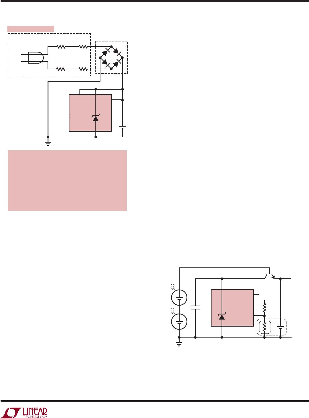
A photovoltaic (PV) application for the LTC4070 is illus-
trated in Figure 6. In this application, transistor Q1 has
been added to further reduce the already low quiescent
current of the LTC4070 to achieve extremely low battery
discharge when the PV cells are not charging the battery.
In long battery life applications, Q1 isolates the battery
from the LTC4070 when Q1’s base voltage falls. Under
normal operation, the PV cells provide current through the
V
BE
and V
BC
diodes of Q1. While the battery is charging,
the majority of PV current flows to the battery. When V
CC
reaches the programmed float voltage, in this case 4.1V
with ADJ floating, then the LTC4070 shunts base-collector
junction current from Q1, effectively reducing the battery
charging current to zero and saturating Q1. In the event
that the thermistor temperature rises and the float voltage
drops, the LTC4070 shunts more current, and Q1 is forced
to operate in reverse active mode until the battery voltage
falls. Once equilibrium is achieved, the difference between
V
BAT
and V
CC
should be less than a few mV, depending on
the magnitude of the shunt current.
Add a series input resistor, R
IN
, to limit the current from
high current solar cells. Solar cells are limited in current
normally, so for small cells no resistor is needed. With
high current PV cells, select R
IN
taking into account the
PV cell’s open-circuit voltage and short-circuit current,
the temperature coefficient of the V
BC
and V
BE
diodes and
the maximum collector current and operating junction
temperature of Q1. Using an isolating transistor reduces
discharge current to a few nanoamps, and may be extended
to other applications as well.
The PV application schematic in Figure 6 also illustrates
using the LTC4070 with a 10k, 5% curve 2 type NTC
thermistor, NTHS0402N02N1002F. Here R
NOM
is 10k,
and the rising temperature trip points are 40°C, 50°C,
60°C and 70°C.
Figure 6. Photovoltaic Charger with Extremely
Low Leakage When Not Charging
Figure 5. 4.2V AC Line Charging, UL Leakage Okay
FLOAT
IF NOT
NEEDED
4070 F05
LTC4070
AC 110
DANGER! HIGH VOLTAGE!
GND
NTCBIAS
MB4S
NTC
Li-Ion
BATTERY
V
CC
R3
249k
R1
249k
ADJ
+
R4
249k
R2
249k
+
DANGEROUS AND LETHAL POTENTIALS ARE PRESENT IN AC
LINE-CONNECTED CIRCUITS! BEFORE PROCEEDING ANY FURTHER,
THE READER IS WARNED THAT CAUTION MUST BE USED IN THE
CONSTRUCTION, TESTING AND USE OF AC LINE-CONNECTED
CIRCUITS. EXTREME CAUTION MUST BE USED IN WORKING WITH
AND MAKING CONNECTIONS TO THESE CIRCUITS. ALL TESTING
PERFORMED ON AN AC LINE-CONNECTED CIRCUIT MUST BE DONE
WITH AN ISOLATION TRANSFORMER CONNECTED BETWEEN THE
AC LINE AND THE CIRCUIT. USERS AND CONSTRUCTORS OF AC
LINE-CONNECTED CIRCUITS MUST OBSERVE THIS PRECAUTION
WHEN CONNECTING TEST EQUIPMENT TO THE CIRCUIT TO AVOID
ELECTRIC SHOCK.
4070 F06
LTC4070
ADJ
R
NTC
: NTHS0402N02N1002F 10k
GND
FLOAT
Q1
MP5650
T
R
NOM
10k
Li-Ion
NTCBIAS
NTC
V
CC
V
BAT
OR 2N3904
C
IN
0.1µF
+
+
+
LTC4070
12
4070fc
Typical applicaTions
The LTC4070 status pins have sufficient drive strength to
use with an LED, for a visual indication of charging status.
Consider the application in Figure 7, where red LED D1 is
connected to the LBO pin and turns off when the battery
voltage is below V
LBTH
. Note that LED D1 discharges the
battery until V
CC
falls below V
LBTH
. Green LED D2, connected
to the HBO pin turns on while the battery is charging. When
the battery voltage rises to within V
HBTH
of the float voltage
including NTC qualification, V
FLOAT_EFF
, D2 turns off to
indicate that the battery is no longer charging. Optionally,
a low leakage diode D3 is placed between the cathode of
D2 and the battery. This diode stops D2 from discharging
the battery when the input supply is not present.
In this application, R
IN
= 205Ω, is sized for a maximum
shunt current of 50mA that occurs at the maximum input
voltage of 15V and the minimum NTC qualified float voltage
Figure 7. Single Cell Charger with LED Status and
NTC Qualified Float Voltage
of 3.8V, assuming the voltage drop on diode D3 is 1.1V.
Without the optional D3, R
IN
increases to 226Ω.
Figure 8 illustrates an application to replace three NiMH cells
with a single Li-Ion cell. This simple application replaces
the NiMH charging solution without the need for a charge
termination or cell balancing scheme. NiMH charging can
be done without termination, but that algorithm limits the
charge rate to C/10. The LTC4070 application allows the
Li-Ion battery to be charged faster without concern of
over-charging.
Figure 9, 12V Wall Adapter Charging with 205mA, il-
lustrates the use of an external PFET transistor to boost
the maximum shunt current. If the battery voltage is
3.6V the battery receives the full charge current of
about 205mA. If the battery temperature is below 40°C,
the float voltage rises to 4.1V (ADJ = floating) then Q1
and the LTC4070 shunts 192mA away from the battery.
If the battery temperature rises, the shunt current increases
to regulate the float voltage 75mV lower per 10°C rise in
battery temperature, as described in Table 1. At a maximum
shunt current of 200mA the minimum float voltage is held
at 3.8V when the battery temperature is above 70°C.
This example illustrates an alternative use of a LED, D1, to
observe the HBO status pin. This LED turns on to provide
a visual indication that the battery is fully charged, and
shunts about 1.5mA when the battery rises to within 40mV
of the desired float voltage. LED D1 discharges the battery,
when no supply is present, until V
CC
falls by more than
V
HBTH
+ V
HBHY
below the float voltage. When using an
LED with the HBO pin in this configuration, it is important
to limit the LED current with a resistor, R
LED
as shown.
Otherwise the step in current through R
IN
that occurs when
the LED turns on may pull V
CC
below the HBO hysteresis.
To prevent that situation, the ratio of R
IN
to R
LED
should
be selected to meet the following relation:
R
IN
R
LED
V
CC
V
LED
(
)
< V
HBHY
50mV
where V
LED
is the forward voltage drop of the LED and a
margin of 50mV is subtracted from the HBO hysteresis.
A V
LED
value of 1.1V is assumed for this example. Refer
to the LED data sheet for the forward voltage drop at the
applied current level.
Figure 8. Replace Three NiMH with Lithium
4070 F07
LTC4070
ADJ
HBO
LBO
D1
LTST
C190CKT
OPTIONAL
D3
BAS416
V
IN
= 8V TO 15V
D2
LTST
C190GKT
R
NTC
: NTHS0402N02N1002F 10k
GND
FLOAT
T
R
NOM
10k
Li-Ion
NTCBIAS
NTC
V
CC
V
BAT
= 4.1V
R
LED1
1k
R
LED2
1k
R
IN
205Ω
1W
+
4070 TA01a
LTC4070
ADJFLOAT
LBO
HBO
GND
T
R
NOM
10k
Li-Ion
NTCBIAS
DRV
NTC
V
CC
I
IN
= 500mA
+
R
NTC
= NTHS0402N02N1002F 10k
V
BAT
= 4.1V
Q1
DMP3015LSS

LTC4070EDDB#TRMPBF

Mfr. #:
Manufacturer:
Analog Devices / Linear Technology
Description:
Battery Management Simple Low-IQ Battery Charger/Protector with NTC Thermistor Input
Lifecycle:
New from this manufacturer.
Delivery:
DHL FedEx Ups TNT EMS
Payment:
T/T Paypal Visa MoneyGram Western Union