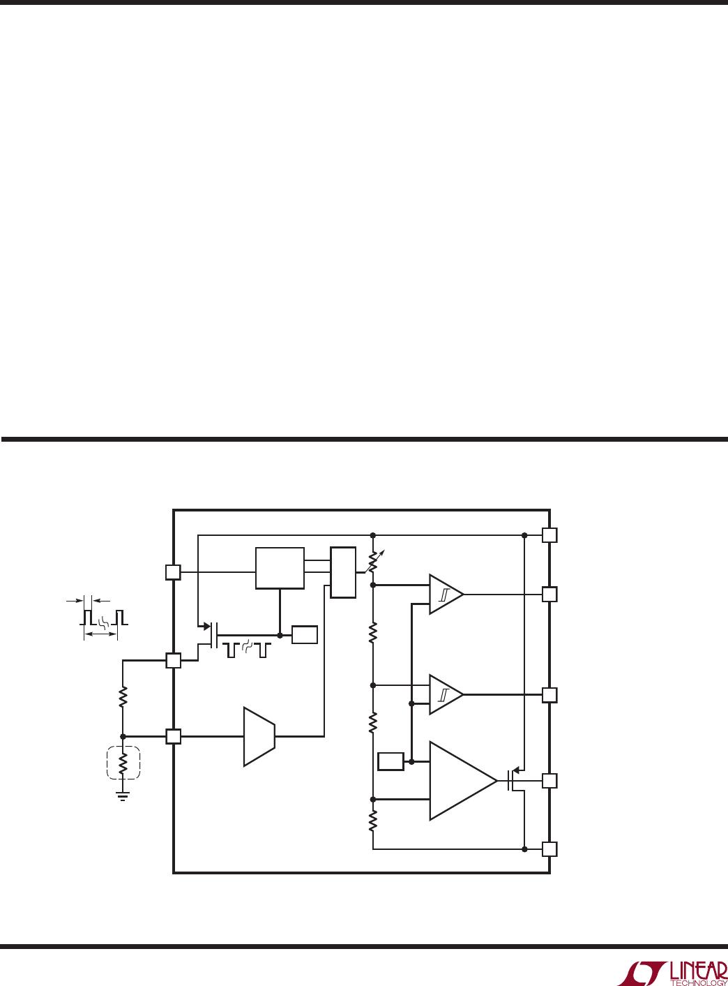
LTC4070
4
4070fc
Typical perForMance characTerisTics
I
CCQ
vs Temperature (ADJ = V
CC
)
V
HBTH
V
CC
Rising vs Temperature
(ADJ = V
CC
)
V
FLOAT
vs Temperature, I
CC
= 1mA
V
FLOAT
vs NTC Temperature,
I
CC
= 1mA
V
LBTH
V
CC
Falling vs Temperature V
LBHY
vs Temperature
Battery Discharge I
CC
vs V
CC
Load Regulation DV
FLOAT
vs I
CC
T
A
= 25°C, unless otherwise noted.
V
HBHY
vs Temperature
(ADJ = V
CC
)
V
CC
(V)
I
CC
(nA)
1000
900
700
800
600
500
400
300
200
100
0
1
0
2
4070 G01
3 4
FALLING
ADJ = GND
RISING
I
CC
(mA)
V
FLOAT
(mV)
10
9
7
8
6
5
4
3
2
1
0
10
0
20 30
4070 G02
40 50 60
TEMPERATURE (°C)
V
FLOAT
(V)
4.30
4.25
4.15
4.20
4.10
4.05
4.00
3.95
3.90
–25
–50
25 500
4070 G03
75 100 125
ADJ = V
CC
ADJ = FLOAT
ADJ = GND
NO NTC
TEMPERATURE (°C)
I
CCQ
(nA)
1000
900
700
800
600
500
400
300
200
100
0
–25
–50
25 500
4070 G04
75 100 125
TEMPERATURE (°C)
V
HBTH
(mV)
100
90
70
80
60
50
40
30
20
10
0
–25
–50
25 500
4070 G05
75 100 125
TEMPERATURE (°C)
V
HBHY
(mV)
300
250
150
200
100
50
0
–25
–50
25 500
4070 G06
75 100 125
TEMPERATURE (°C)
V
FLOAT
(V)
4.3
4.2
4.0
4.1
3.9
3.8
3.7
4020
0
60
4070 G07
80 100
ADJ = V
CC
ADJ = FLOAT
ADJ = GND
TEMPERATURE (°C)
V
LBTH
(V)
3.250
3.245
3.235
3.240
3.225
3.230
3.210
3.205
3.220
3.215
3.200
–25
–50
25 500
4070 G08
75 100 125
ADJ = FLOAT
ADJ = GND
ADJ = V
CC
TEMPERATURE (°C)
V
LBHY
(V)
320
300
240
220
280
260
200
–25
–50
25 500
4070 G09
75 100 125
ADJ = FLOAT
ADJ = GND
ADJ = V
CC
LTC4070
5
4070fc
Typical perForMance characTerisTics
Hot Plug Transient, C
C
= 330µF,
R
IN
= 81Ω
Step Response with 800mAHr
Battery, R
IN
= 81Ω
V
OH
LBO/HBO vs I
SOURCE
V
OL
LBO/HBO vs I
SINK
Power Spectral Density
T
A
= 25°C, unless otherwise noted.
I
SOURCE
(mA)
V
CC
– V
OH
(V)
2.5
1.5
2.0
1.0
0.5
0
1.50.5 1.0
0
2.0
4070 G10
2.5 3.0
LBO
V
CC
= 3.1V
HBO
V
CC
= V
F
– 25m
I
SINK
(mA)
V
OL
(V)
2.5
1.5
2.0
1.0
0.5
0
42
0
6
4070 G11
8 10
V
CC
= 3.7V
4ms/DIV
4070 G13
CH1 = V
IN
(2V/DIV)
CH2 = V
CC
(2V/DIV)
CH3 = V
HBO
(2V/DIV)
CH4 = I
IN
(10mA/DIV)
400ns/DIV
CH1 = V
IN
(2V/DIV)
CH2 = V
CC
(2V/DIV)
CH3 = V
HBO
(2V/DIV)
CH4 = I
IN
(10mA/DIV)
4070 G14
FREQUENCY (Hz)
PSD (µV
RMS
/√Hz)
35
25
30
20
15
10
5
0
101 100
0
1000 10000
4070 G12
100000
C
C
= 10µF, I
CC
= 1mA, 1Hz Res
Bandwidth, Noise = 1.0452mV
RMS
from 10Hz to 100kHz
pin FuncTions
NTCBIAS (Pin 1): NTC Bias Pin. Connect a resistor from
NTCBIAS to NTC, and a thermistor from NTC to GND. Float
NTCBIAS when not in use. Minimize parasitic capacitance
on this pin.
NTC (Pin 2): Input to the Negative Temperature Coefficient
Thermistor Monitoring Circuit. The NTC pin connects to
a negative temperature coefficient thermistor which is
typically co-packaged with the battery to determine the
temperature of the battery. If the battery temperature is too
high, the float voltage is reduced. Connect a low drift bias
resistor from NTCBIAS to NTC and a thermistor from NTC
to GND. When not in use, connect NTC to V
CC
. Minimize
parasitic capacitance on this pin.
ADJ (Pin 3): Float Voltage Adjust Pin. Connect ADJ to GND
to program 4.0V float voltage. Disconnect ADJ to program
4.1V float voltage. Connect ADJ to V
CC
to program 4.2V
float voltage. The float voltage is also adjusted by the NTC
thermistor.
LTC4070
6
4070fc
block DiagraM
pin FuncTions
4070 BD
3-STATE
DETECT
OSC
CLK
ADJ
1.5s
PULSED
DUTY CYCLE < 0.002%
30µs
NTCBIAS
NTC
R
NOM
10k
T
+
+
REF
+
EA
GND
DRV
HBO
LBO
V
CC
ADC
LTC4070
HBO (Pin 4): High Battery Monitor Output (Active High).
HBO is a CMOS output that indicates that the battery is
almost fully charged and current is being shunted away
from BAT. This pin is driven high when V
CC
rises to within
V
HBTH
of the effective float voltage. The absolute value of
this threshold depends on ADJ and NTC, both of which
affect the float voltage. HBO is driven low when V
CC
falls
by more than (V
HBTH
+ V
HBHY
) below the float voltage.
Refer to Table 1 for the effective float voltage.
GND (Pin 5, Exposed Pad Pin 9): Ground. The exposed
package pad must be connected to PCB ground for rated
thermal performance.
LBO (Pin 6): Low Battery Monitor Output (Active High).
LBO is a CMOS output that indicates when the battery
is discharged below 3.2V or rises above 3.5V. This pin
is driven high if V
CC
< V
LBTH
, and is driven low if V
CC
>
(V
LBTH
+ V
LBHY
).
DRV (Pin 7): External Drive Output. Connect to the gate of
an external PFET to increase shunt current for applications
which require more than 50mA charge current. Minimize
capacitance and leakage current on this pin. When not in
use, float DRV.
V
CC
(Pin 8): Input Supply Pin. The input supply voltage is
regulated to 4.0V, 4.1V, or 4.2V depending on the ADJ pin
state (see the ADJ pin description for more detail). This pin
can sink up to 50mA in order to keep the voltage regulation
within accuracy limits. When no battery is present, decouple
to GND with a capacitor, C
IN
, of at least 0.1µF.

LTC4070EDDB#TRMPBF

Mfr. #:
Manufacturer:
Analog Devices / Linear Technology
Description:
Battery Management Simple Low-IQ Battery Charger/Protector with NTC Thermistor Input
Lifecycle:
New from this manufacturer.
Delivery:
DHL FedEx Ups TNT EMS
Payment:
T/T Paypal Visa MoneyGram Western Union