XC18V00 Series In-System-Programmable Configuration PROMs
DS026 (v5.2) January 11, 2008 www.xilinx.com
Product Specification 16
Recommended Operating Conditions
Quality and Reliability Characteristics
DC Characteristics Over Operating Conditions
Symbol Parameter Min Max Units
V
CCINT
Internal voltage supply 3.0 3.6 V
V
CCO
Supply voltage for output drivers for 3.3V operation 3.0 3.6 V
Supply voltage for output drivers for 2.5V operation 2.3 2.7 V
V
IL
Low-level input voltage 0 0.8 V
V
IH
High-level input voltage 2.0 5.5 V
V
O
Output voltage 0 V
CCO
V
T
VCC
V
CCINT
rise time from 0V to nominal voltage
(1)
150ms
T
A
Operating ambient temperature
(2)
–40 85 ° C
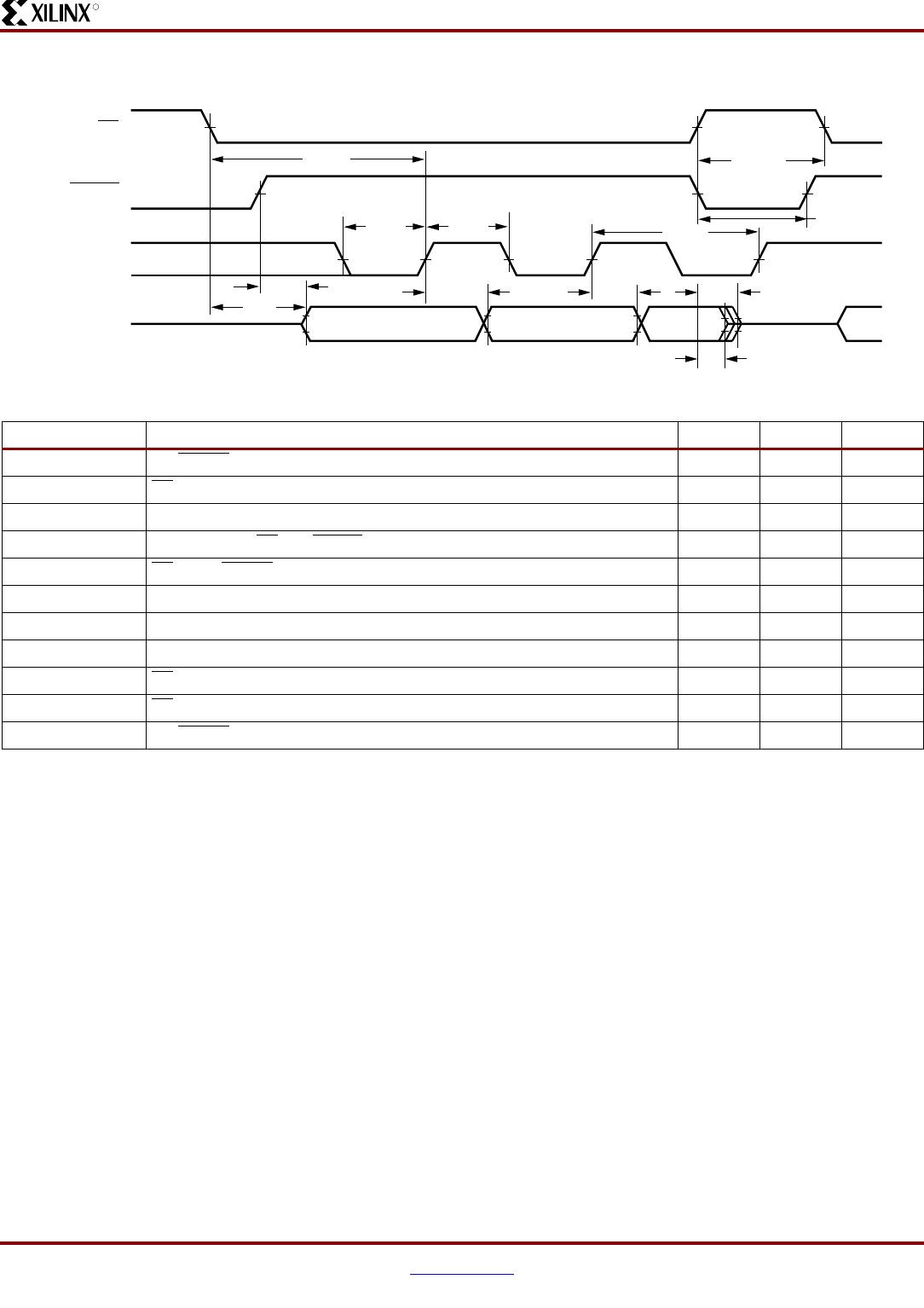
Notes:
1. At power up, the device requires the V
CCINT
power supply to rise monotonically from 0V to nominal voltage within the specified V
CCINT
rise
time. If the power supply cannot meet this requirement, then the device might not perform power-on-reset properly. See Figure 9, page 14.
2. Covers the industrial temperature range.
Symbol Description Min Max Units
T
DR
Data retention 20 – Years
N
PE
Program/erase cycles (Endurance) 20,000 – Cycles
V
ESD
Electrostatic discharge (ESD) 2,000 – Volts
Symbol Parameter Test Conditions Min Max Units
V
OH
High-level output voltage for 3.3V outputs I
OH
= –4 mA 2.4 – V
High-level output voltage for 2.5V outputs I
OH
= –500 μA90% V
CCO
–V
V
OL
Low-level output voltage for 3.3V outputs I
OL
= 8 mA – 0.4 V
Low-level output voltage for 2.5V outputs I
OL
= 500 μA–0.4V
I
CC
Supply current, active mode 25 MHz – 25 mA
I
CCS
Supply current, standby mode – 10 mA
I
ILJ
JTAG pins TMS, TDI, and TDO pull-up current
(1)
V
CCINT
= MAX
V
IN
= GND
–100μA
I
IL
Input leakage current V
CCINT
= Max
V
IN
= GND or V
CCINT
–10 10 μA
I
IH
Input and output high-Z leakage current V
CCINT
= Max
V
IN
= GND or V
CCINT
–10 10 μA
C
IN
Input capacitance V
IN
= GND
f = 1.0 MHz
–8pF
C
OUT
Output capacitance
V
OUT
= GND
f = 1.0 MHz
–
14 pF
Notes:
1. Internal pull-up resistors guarantee valid logic levels at unconnected input pins. These pull-up resistors do not guarantee valid logic levels
when input pins are connected to other circuits.