25LCXXX
DS22131C-page 10 Preliminary © 2009 Microchip Technology Inc.
FIGURE 3-2: BYTE WRITE SEQUENCE
FIGURE 3-3: PAGE WRITE SEQUENCE
SO
SI
CS
91011 2122232425262728293031
0000000115 14 13 12
21076543210
Instruction 16-bit Address Data Byte
High-Impedance
SCK
0 23456718
Twc
SI
CS
9 1011 2122232425262728293031
0000000115 14 13 12
21076543210
Instruction 16-bit Address Data Byte 1
SCK
0 2345671
8
SI
CS
41 42 43 46 47
76543210
Data Byte n (16/32/64 max)
SCK
32 34 35 36 37 38 3933
40
76543210
Data Byte 3
76543210
Data Byte 2
44 45
© 2009 Microchip Technology Inc. Preliminary DS22131C-page 11
25LCXXX
3.4 Write Enable (WREN) and Write
Disable (WRDI)
The 25LCXXX contains a write enable latch. See
Table 5-1 for the write-protect functionality matrix. This
latch must be set before any write operation will be com-
pleted internally. The WREN instruction will set the latch,
and the WRDI will reset the latch.
The following is a list of conditions under which the
write enable latch will be reset:
Power-up
WRDI instruction successfully executed
WRSR instruction successfully executed
WRITE instruction successfully executed
FIGURE 3-4: WRITE ENABLE SEQUENCE (WREN)
FIGURE 3-5: WRITE DISABLE SEQUENCE (WRDI)
SCK
0 2345671
SI
High-Impedance
SO
CS
010000 01
SCK
0 2345671
SI
High-Impedance
SO
CS
010000 01
0
25LCXXX
DS22131C-page 12 Preliminary © 2009 Microchip Technology Inc.
3.5 Read Status Register Instruction
(RDSR)
The Read Status Register instruction (RDSR) provides
access to the STATUS register. The STATUS register
may be read at any time, even during a write cycle. The
STATUS register is formatted as follows:
TABLE 3-2: STATUS REGISTER
The Write-In-Process (WIP) bit indicates whether the
25LCXXX is busy with a write operation. When set to a
1’, a write is in progress, when set to a ‘0’, no write is
in progress. This bit is read-only.
The Write Enable Latch (WEL) bit indicates the status
of the write enable latch and is read-only. When set to
a ‘
1’, the latch allows writes to the array, when set to a
0’, the latch prohibits writes to the array. The state of
this bit can always be updated via the WREN or WRDI
commands regardless of the state of write protection
on the STATUS register. These commands are shown
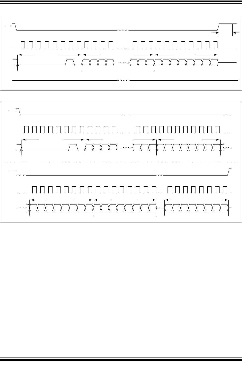
in Figure 3-4 and Figure 3-5.
The Block Protection (BP0 and BP1) bits indicate
which blocks are currently write-protected. These bits
are set by the user issuing the WRSR instruction. These
bits are nonvolatile, and are shown in Table 3-3.
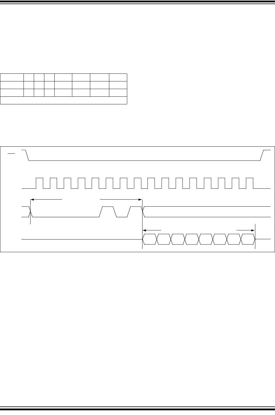
See Figure 3-6 for the RDSR timing sequence.
FIGURE 3-6: READ STATUS REGISTER TIMING SEQUENCE (RDSR)
7 654 3 2 1 0
W/R –––W/RW/R R R
WPEN X X X BP1 BP0 WEL WIP
W/R = writable/readable. R = read-only.
SO
SI
CS
9101112131415
11000000
7654 210
Instruction
Data from STATUS Register
High-Impedance
SCK
0 2345671
8
3

25LC256T-H/SN

Mfr. #:
Manufacturer:
Microchip Technology
Description:
EEPROM 256K, 32K X 8, 2.5V SER EE 150C
Lifecycle:
New from this manufacturer.
Delivery:
DHL FedEx Ups TNT EMS
Payment:
T/T Paypal Visa MoneyGram Western Union