© 2009 Microchip Technology Inc. Preliminary DS22131C-page 9
25LCXXX
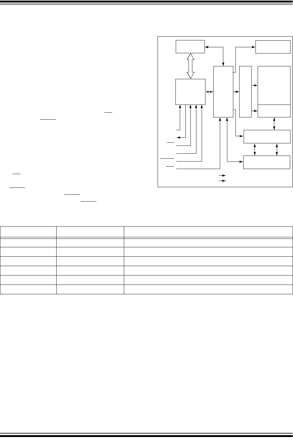
3.2 Read Sequence
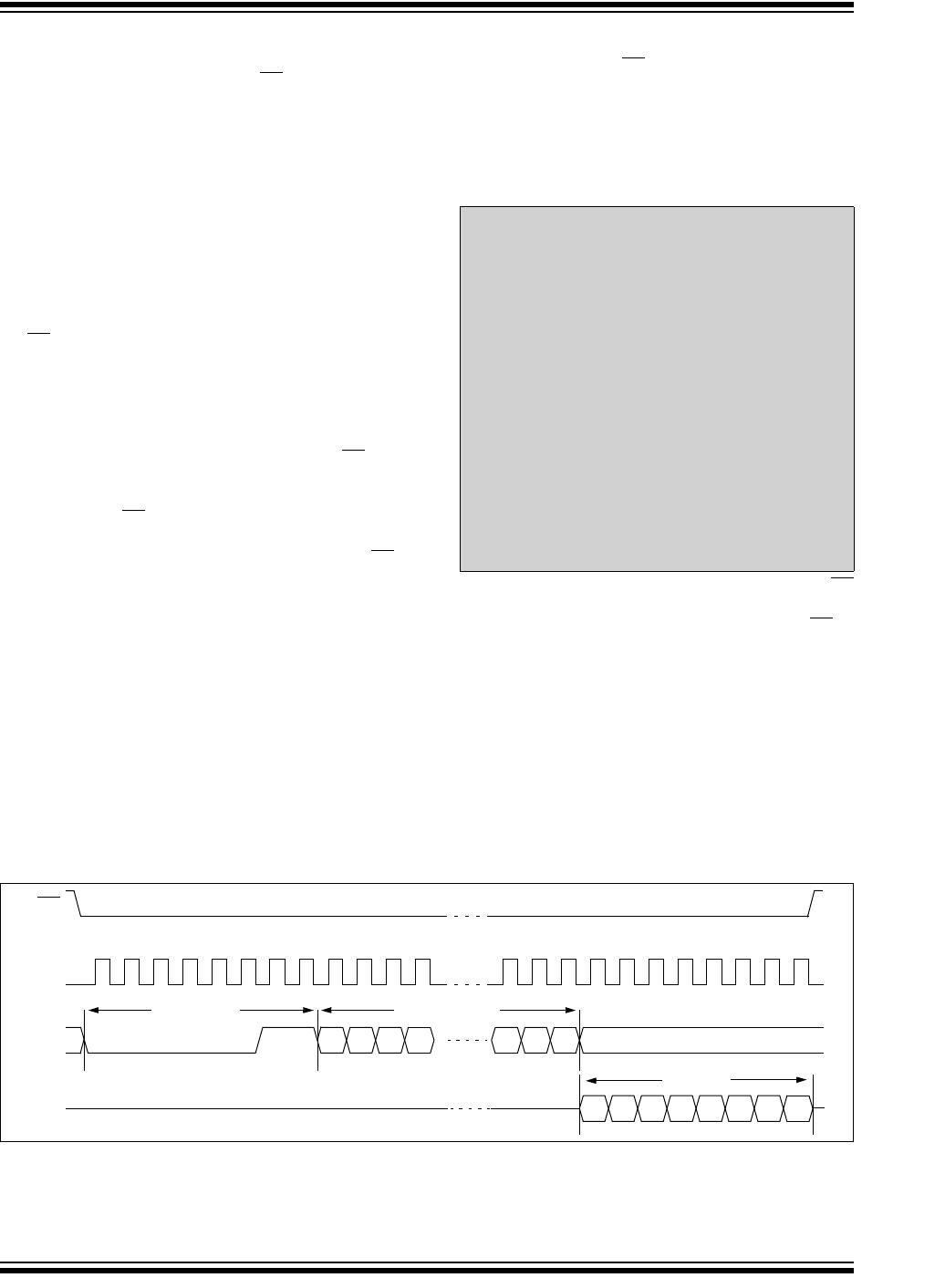
The device is selected by pulling CS low. The 8-bit
READ instruction is transmitted to the 25LCXXX fol-
lowed by the 16-bit address. After the correct READ
instruction and address are sent, the data stored in the
memory at the selected address is shifted out on the
SO pin. The data stored in the memory at the next
address can be read sequentially by continuing to pro-
vide clock pulses. The internal Address Pointer is auto-
matically incremented to the next higher address after
each byte of data is shifted out. When the highest
address is reached, the address counter rolls over to
address 0000h allowing the read cycle to be continued
indefinitely. The read operation is terminated by raising
the CS
pin (Figure 3-1).
3.3 Write Sequence
Prior to any attempt to write data to the 25LCXXX, the
write enable latch must be set by issuing the WREN
instruction (Figure 3-4). This is done by setting CS low
and then clocking out the proper instruction into the
25LCXXX. After all eight bits of the instruction are
transmitted, the CS
must be brought high to set the
write enable latch. If the write operation is initiated
immediately after the WREN instruction without CS
being brought high, the data will not be written to the
array because the write enable latch will not have been
properly set.
Once the write enable latch is set, the user may
proceed by setting the CS
low, issuing a WRITE instruc-
tion, followed by the 16-bit address, and then the data
to be written. Depending upon the density, a page of
data that ranges from 16 bytes to 64 bytes can be sent
to the device before a write cycle is necessary. The only
restriction is that all of the bytes must reside in the
same page.
For the data to be actually written to the array, the CS
must be brought high after the Least Significant bit (D0)
of the n
th
data byte has been clocked in. If CS is
brought high at any other time, the write operation will
not be completed. Refer to Figure 3-2 and Figure 3-3
for more detailed illustrations on the byte write
sequence and the page write sequence, respectively.
While the write is in progress, the STATUS register may
be read to check the status of the WPEN, WIP, WEL,
BP1 and BP0 bits (Figure 3-6). A read attempt of a
memory array location will not be possible during a
write cycle. When the write cycle is completed, the
write enable latch is reset.
FIGURE 3-1: READ SEQUENCE
Note: Page write operations are limited to writing
bytes within a single physical page,
regardless of the number of bytes
actually being written. Physical page
boundaries start at addresses that are
integer multiples of the page buffer size (or
‘page size’) and, end at addresses that are
integer multiples of page size – 1. If a
Page Write command attempts to write
across a physical page boundary, the
result is that the data wraps around to the
beginning of the current page (overwriting
data previously stored there), instead of
being written to the next page as might be
expected. It is therefore necessary for the
application software to prevent page write
operations that would attempt to cross a
page boundary.
SO
SI
SCK
CS
0 234567891011 21222324252627282930311
0100000115 14 13 12 210
76543210
Instruction 16-bit Address
Data Out
High-Impedance