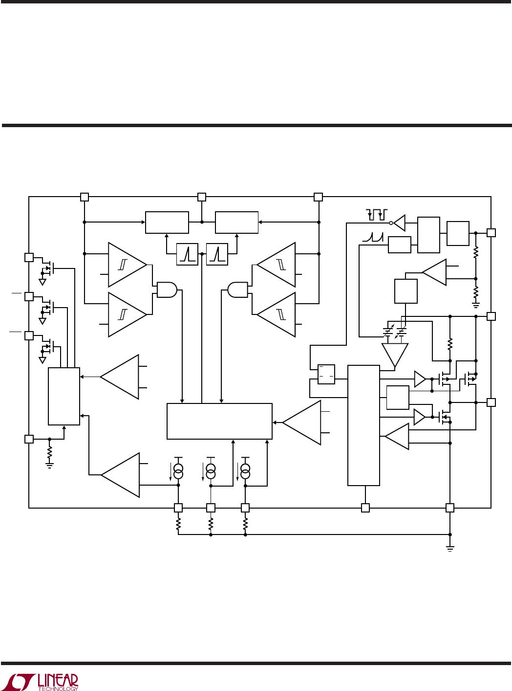
LTC3550-1
10
35501f
PI FU CTIO S
UUU
USBIN (Pin 1): USB Input Supply Pin. Provides power to
the battery charger. The maximum supply current is 650mA.
This should be bypassed with a 1µF capacitor.
IUSB (Pin 2): USB Charge Current Program and Monitor
Pin. The charge current can be set by connecting a resis-
tor, R
IUSB
, to ground. When charging in constant-current
mode, this pin servos to 1V. The voltage on this pin can
be used to measure the charge current delivered from the
USB input using the following formula:
I
V
R
BAT
IUSB
IUSB
= 1000
ITERM (Pin 3): Termination Current Threshold Program
Pin. The current termination threshold, I
TERMINATE
, can be
set by connecting a resistor, R
ITERM
, to ground. I
TERMINATE
is set by the following formula:
I
V
R
TERMINATE
ITERM
=
100
When the charge current, I
BAT
, falls below the termination
threshold, charging stops and the
C
H
R
G output becomes
high impedance.
This pin is internally clamped to approximately 1.5V. Driv-
ing this pin to voltages beyond the clamp voltage should
be avoided.
P
W
R (Pin 4): Open-Drain Power Supply Status Output.
When the DCIN or USBIN pin voltage is suffi cient to
begin charging (i.e., when the supply is greater than
the undervoltage lockout threshold and at least 180mV
above the battery terminal), the
P
W
R pin is pulled low by
an internal N-channel MOSFET. Otherwise,
P
W
R is high
impedance. The output is capable of sinking up to 10mA,
making it suitable for driving an LED.
C
H
R
G (Pin 5): Open-Drain Charge Status Output. When
the LTC3550-1 is charging, the
C
H
R
G pin is pulled low by
an internal N-channel MOSFET. When the charge cycle is
completed,
C
H
R
G becomes high impedance. This output
is capable of sinking up to 10mA, making it suitable for
driving an LED.
V
OUT
(Pin 6): Output Voltage Feedback Pin. Receives the
feedback voltage from the buck regulator output.
V
CC
(Pin 7): Buck Regulator Input Supply Pin. Must be
closely decoupled to GND (Pins 8, 9) with a 2.2µF or
greater ceramic capacitor.
GND (Pins 8, 9): Ground.
SW (Pin 10): Switch Node Connection to Inductor. This
pin connects to the drains of the internal main (top) and
synchronous (bottom) power MOSFET switches.
RUN (Pin 11): Buck Regulator Run Control Input. Forcing
this pin above 1.5V enables the regulator. Forcing this pin
below 0.3V shuts it down. In shutdown, all buck regulator
functions are disabled drawing <1µA supply current from
V
CC
. Do not leave RUN fl oating.
ENABLE (Pin 12): Charger Enable Input. When the
LTC3550-1 is charging from the DCIN source, a logic low
on this pin enables the charger. When the LTC3550-1 is
charging from the USBIN source, a logic high on this pin
enables the charger. If this input is left fl oating, an internal
2MΩ pulldown resistor defaults the LTC3550-1 to charge
when a wall adapter is applied and to shut down if only
the USB source is applied.
USBPWR (Pin 13): Open-Drain USB Power Status Output.
When the voltage on the USBIN pin is suffi cient to begin
charging and there is insuffi cient power at DCIN, the
USBPWR pin is high impedance. In all other cases, this pin
is pulled low by an internal N-channel MOSFET, provided
that there is power present at DCIN, USBIN, or BAT inputs.
This output is capable of sinking up to 1mA, making it
suitable for driving high impedance logic inputs.
IDC (Pin 14): Wall Adapter Charge Current Program and
Monitor Pin. The charge current is set by connecting a
resistor, R
IDC
, to ground. When charging in constant-
current mode, this pin servos to 1V. The voltage on this
pin can be used to measure the charge current using the
following formula:
I
V
R
BAT
IDC
IDC
= 1000
BAT (Pin 15): Charger Output. This pin provides charge
current to the battery and regulates the fi nal fl oat voltage
to 4.2V.
LTC3550-1
11
35501f
PI FU CTIO S
UUU
DCIN (Pin 16): Wall Adapter Input Supply Pin. Provides
power to the battery charger. The maximum supply
current is 950mA. This should be bypassed with a 1µF
capacitor.
Exposed Pad (Pin 17): GND. The exposed backside of the
package is ground and must be soldered to the PCB ground
for electrical connection and maximum heat transfer.
BLOCK DIAGRA
W
FREQ
SHIFT
13
+
+
+
+
TERM
RECHRG
LOGIC
4.1V
BAT
3.95V
BAT
100mV
I
BAT
/1000
I
BAT
/1000
I
BAT
/1000
4
5
12
3 14 2 11
DC_ENABLE USB_ENABLE
CHARGER CONTROL
CC/CV
REGULATOR
CC/CV
REGULATOR
1516 1
R
ITERM
R
IUSB
R
IDC
ITERM IUSBIDC
105°C
T
DIE
USB
SOFT-
START
DC
SOFT-
START
USBIN UVLODCIN UVLO
DCIN BAT USBIN
USBPWR
ENABLE
PWR
CHRG
TERMINATION
RECHARGE
THERMAL
REGULATION
1mA MAX
10mA MAX
10mA MAX
3550-1 BD
+
+
+
4.15V
BAT
+
I
RCMP
+
I
COMP
V
CC
S
R
RS LATCH
SWITCHING
LOGIC
AND
BLANKING
CIRCUIT
ANTI-
SHOOT-
THRU
+
EA
BURST
CLAMP
Q
Q
5
7
V
OU
T
6
SW
10
R2
R1
0.6V
SLOPE
COMP
OSC
RUN 8, 9, 17
GND
I
TH
R
ENABLE
LTC3550-1
12
35501f
OPERATIO
U
The LTC3550-1 consists of two main blocks: a lithium-ion
battery charger and a high-effi ciency buck converter that
can be powered from the battery. The charger is designed
to effi ciently manage charging of a single-cell lithium-ion
battery from two separate power sources: a wall adapter
and USB power bus. The internal P-channel MOSFETs
can supply up to 950mA from the wall adapter source
and 500mA from the USB power source. The fi nal oat
voltage accuracy is ±0.6%.
The buck converter uses a constant frequency, current
mode step-down architecture. Both the main (P-channel
MOSFET) and synchronous (N-channel MOSFET) switches
for the buck converter are internal. The LTC3550-1 requires
no external diodes or sense resistors.
Lithium-Ion Battery Charger
A charge cycle begins when the voltage at either the DCIN
pin or USBIN pin rises above the UVLO threshold level and
the charger is enabled through the ENABLE pin. The “on”
state of this pin depends on which source is supplying
power. When the wall adapter input (DCIN) is supply-
ing power, logic low enables the charger and logic high
disables it (a 2MΩ pulldown defaults the charger to
the charging state). The opposite is true when the USB
Figure 1. LTC3550-1 State Diagram of a Charge Cycle
input (USBIN) is supplying power; logic low disables the
charger and logic high enables it (the default is the
shutdown state). The DCIN input draws 20µA when the
charger is in shutdown. The USBIN input draws 18µA dur-
ing shutdown if no power is applied to DCIN, but draws
only 10µA when V
DCIN
> V
USBIN
.
Once the charger is enabled, it enters constant-current
mode, where the programmed charge current is supplied
to the battery. When the BAT pin approaches the fi nal
oat voltage (4.2V), the charger enters constant-voltage
mode and the charge current begins to decrease. Once
the charge current drops below the programmed termina-
tion threshold (set by the external resistor R
ITERM
), the
internal P-channel MOSFET is shut off and the charger
enters standby mode.
In standby mode, the charger sits idle and monitors the
battery voltage using a comparator with a 6ms fi lter time
(t
RECHRG
). A charge cycle automatically restarts when the
battery voltage falls below 4.1V (which corresponds to ap-
proximately 80% to 90% battery capacity). This ensures
that the battery is kept near a fully charged condition and
eliminates the need for periodic charge cycle initiations.
Figure 1 uses a state diagram to describe the behavior of
the LTC3550-1 battery charger.
SHUTDOWN
MODE
I
USBIN
DROPS TO 18µA
CHRG STATE: Hi-Z
CHARGE
MODE
FULL CURRENT
CHRG STATE: PULLDOWN
CHARGE
MODE
FULL CURRENT
CHRG STATE: PULLDOWN
STANDBY
MODE
NO CHARGE CURRENT
CHRG STATE: Hi-Z
SHUTDOWN
MODE
I
DCIN
DROPS TO 20µA
CHRG STATE: Hi-Z
BAT < 4.1VBAT < 4.1V
I
BAT
< I
TERMINATE
IN VOLTAGE MODE
I
BAT
< I
TERMINATE
IN VOLTAGE MODE
POWER SELECTION
STANDBY
MODE
NO CHARGE CURRENT
CHRG STATE: Hi-Z
ENABLE
DRIVEN LOW
ENABLE
DRIVEN LOW
ENABLE
DRIVEN HIGH
DCIN POWER
REMOVED
DCIN POWER
REMOVED
USBIN POWER
REMOVED OR DCIN
POWER APPLIED
USBIN POWER
REMOVED OR
DCIN POWER
APPLIED
DCIN POWER APPLIED ONLY USB POWER APPLIED
STARTUP
3550-1 F01
ENABLE
DRIVEN HIGH

LTC3550EDHC-1#PBF

Mfr. #:
Manufacturer:
Analog Devices / Linear Technology
Description:
Battery Management Dual Input USB/AC Adapter Li-Ion Battery Charger w/ 600mA Buck Converter
Lifecycle:
New from this manufacturer.
Delivery:
DHL FedEx Ups TNT EMS
Payment:
T/T Paypal Visa MoneyGram Western Union

Products related to this Datasheet