LTC3550-1
16
35501f
APPLICATIO S I FOR ATIO
WUU
U
The DC current rating of the inductor should be at least
equal to the maximum load current plus half the ripple
current to prevent core saturation. Thus, a 720mA rated
inductor should be enough for most applications (600mA
+ 120mA). For best effi ciency, choose a low DC-resistance
inductor.
The inductor value also has an effect on Burst Mode opera-
tion. The transition to low current operation begins when
the inductor current peaks fall to approximately 200mA.
Lower inductor values (higher ΔI
L
) will cause this to occur
at lower load currents, which can cause a dip in effi ciency
in the upper range of low current operation. In Burst Mode
operation, lower inductance values will cause the burst
frequency to increase.
Inductor Core Selection
Different core materials and shapes will change the
size/current and price/current relationship of an induc-
tor. Toroid or shielded pot cores in ferrite or permalloy
materials are small and don’t radiate much energy, but
generally cost more than powdered iron core inductors
with similar electrical characteristics. The choice of which
style inductor to use often depends more on the price vs
size requirements and any radiated fi eld/EMI requirements
than on what the LTC3550-1 requires to operate. Table 2
shows some typical surface mount inductors that work
well in LTC3550-1 applications.
Table 2. Representative Surface Mount Inductors
PART
NUMBER
VALUE
(µH)
DCR
(Ω MAX)
MAX DC
CURRENT (A)
SIZE
W × L × H (mm)
Sumida
CDRH3D16
1.5
2.2
3.3
4.7
0.043
0.075
0.110
0.162
1.55
1.20
1.10
0.90
3.8 × 3.8 × 1.8
Sumida
CMD4D06
2.2
3.3
4.7
0.116
0.174
0.216
0.950
0.770
0.750
3.5 × 4.3 × 0.8
Panasonic
ELT5KT
3.3
4.7
0.17
0.20
1.00
0.95
4.5 × 5.4 × 1.2
Murata
LQH32CN
1.0
2.2
4.7
0.060
0.097
0.150
1.00
0.79
0.65
2.5 × 3.2 × 2.0
C
IN
and C
OUT
Selection
In continuous mode, the source current of the top MOSFET
is a square wave of duty cycle V
OUT
/V
CC
. To prevent large
voltage transients, a low ESR input capacitor sized for the
maximum RMS current must be used. The maximum RMS
capacitor current is given by:
C required I I
VVV
V
IN RMS OMAX
OUT CC OUT
CC
()
(2)
This formula has a maximum at V
CC
= 2V
OUT
, where I
RMS
= I
OUT
/2. This simple worst-case condition is commonly
used for design because even signifi cant deviations do not
offer much relief. Note that the capacitor manufacturer’s
ripple current ratings are often based on 2000 hours of
life. This makes it advisable to further derate the capaci-
tor, or choose a capacitor rated at a higher temperature
than required. Always consult the manufacturer if there
is any question.
The selection of C
OUT
is driven by the required effective
series resistance (ESR).
Typically, once the ESR requirement for C
OUT
has been
met, the RMS current rating generally far exceeds the
I
RIPPLE(P-P)
requirement. The output ripple ΔV
OUT
is
determined by:
∆≅ +
VIESR
fC
OUT L
OUT
1
8
(3)
where f = operating frequency, C
OUT
= output capacitance
and ΔI
L
= ripple current in the inductor. For a fi xed output
voltage, the output ripple voltage is highest at maximum
input voltage since ΔI
L
increases with input voltage.
Aluminum electrolytic and solid tantalum capacitors are
both available in surface mount confi gurations. In the case
of tantalum, it is critical that the capacitors are surge tested
for use in switching power supplies. An excellent choice is
the AVX TPS series of surface mount tantalum. These are
specially constructed and tested for low ESR so they give
the lowest ESR for a given volume. Other capacitor types
include Sanyo POSCAP, Kemet T510 and T495 series, and
Sprague 593D and 595D series. Consult the manufacturer
for other specifi c recommendations.
LTC3550-1
17
35501f
APPLICATIO S I FOR ATIO
WUU
U
Using Ceramic Input and Output Capacitors
Higher capacitance values, lower cost ceramic capacitors
are now becoming available in smaller case sizes. Their
high ripple current, high voltage rating and low ESR make
them ideal for switching regulator applications. Because the
LTC3550-1’s control loop does not depend on the output
capacitor’s ESR for stable operation, ceramic capacitors
can be used freely to achieve very low output ripple and
small circuit size.
When choosing the input and output ceramic capacitors,
choose the X5R or X7R dielectric formulations. These
dielectrics have the best temperature and voltage charac-
teristics of all the ceramics for a given value and size.
Effi ciency Considerations
The effi ciency of a switching regulator is equal to the output
power divided by the input power times 100%. It is often
useful to analyze individual losses to determine what is
limiting the effi ciency and which change would produce
the most improvement. Effi ciency can be expressed as:
Effi ciency = 100% – (L1 + L2 + L3 + ...)
where L1, L2, etc. are the individual losses as a percent-
age of input power.
Although all dissipative elements in the circuit produce
losses, two main sources usually account for most of
the losses in LTC3550-1 circuits: V
CC
quiescent current
and I
2
R losses. The V
CC
quiescent current loss dominates
the effi ciency loss at very low load currents whereas the
I
2
R loss dominates the effi ciency loss at medium to high
load currents. In a typical effi ciency plot, the effi ciency
curve at very low load currents can be misleading since
the actual power lost is of no consequence as illustrated
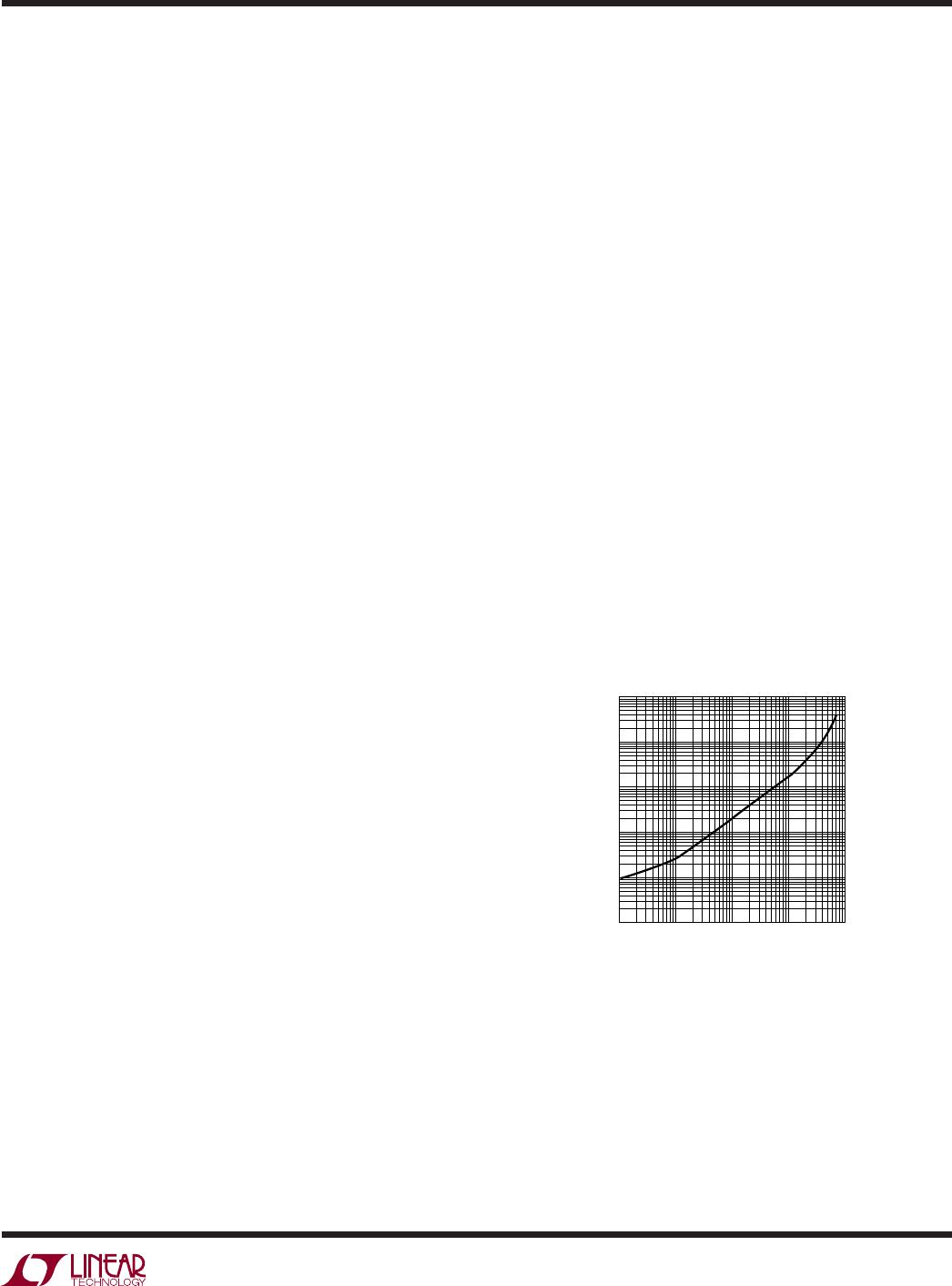
in Figure 3.
1. The V
CC
quiescent current is due to two components:
the DC bias current as given in the Electrical Charac-
teristics and the internal main switch and synchronous
switch gate charge currents. The gate charge current
results from switching the gate capacitance of the
internal power MOSFET switches. Each time the gate
is switched from high to low to high again, a packet of
charge, dQ, moves from V
CC
to ground. The resulting
dQ/dt is the current out of V
CC
that is typically larger
than the DC bias current. In continuous mode, I
GATECHG
= f(Q
T
+ Q
B
) where Q
T
and Q
B
are the gate charges of
the internal top and bottom switches. Both the DC bias
and gate charge losses are proportional to V
CC
and
thus their effects will be more pronounced at higher
supply voltages.
2. I
2
R losses are calculated from the resistances of the
internal switches, R
SW
, and external inductor R
L
. In
continuous mode, the average output current fl owing
through inductor L is “chopped” between the main
switch and the synchronous switch. Thus, the series
resistance looking into the SW pin is a function of both
top and bottom MOSFET R
DS(ON)
and the duty cycle
(DC) as follows:
R
SW
= (R
DS(ON)TOP
)(DC) + (R
DS(ON)BOT
)(1 – DC)
The R
DS(ON)
for both the top and bottom MOSFETs can
be obtained from the Typical Performance Characteristics
curves. Thus, to obtain I
2
R losses, simply add R
SW
to R
L
and multiply the result by the square of the average output
current. Other losses including C
IN
and C
OUT
ESR dissipa-
tive losses and inductor core losses generally account for
less than 2% total additional loss.
LOAD CURRENT (mA)
0.1 1
0.00001
POWER LOSS (W)
0.001
1
10 100 1000
3550-1 F03
0.0001
0.01
0.1
Figure 3. Power Lost vs Load Current
LTC3550-1
18
35501f
APPLICATIO S I FOR ATIO
WUU
U
Thermal Considerations
The battery charger’s thermal regulation feature and the
buck regulator’s high effi ciency make it unlikely that enough
power is dissipated to exceed the LTC3550-1 maximum
junction temperature. Nevertheless, it is a good idea to
do some thermal analysis for worst-case conditions.
The junction temperature, T
J
, is given by: T
J
= T
A
+ T
RISE
where T
A
is the ambient temperature. The temperature
rise is given by:
T
RISE
= P
D
θ
JA
where P
D
is the power dissipated and θ
JA
is the thermal
resistance from the junction of the die to the ambient
temperature.
In most applications the buck regulator does not dissipate
much heat due to its high effi ciency. The majority of the
LTC3550-1 power dissipation occurs when charging a
battery. Fortunately, the LTC3550-1 automatically reduces
the charge current during high power conditions using
a patented thermal regulation circuit. Thus, there is no
need to design for worst-case power dissipation scenarios
because the LTC3550-1 ensures that the battery charger
power dissipation never raises the junction temperature
above a preset value of 105°C. In the unlikely case that
the junction temperature is forced above 105°C (due to
abnormally high ambient temperatures or excessive buck
regulator power dissipation), the battery charge current will
be reduced to zero and thus dissipate no heat. As an added
measure of protection, even if the junction temperature
reaches approximately 150°C, the buck regulator’s power
switches will be turned off and the SW node will become
high impedance.
The conditions that cause the LTC3550-1 to reduce charge
current through thermal feedback can be approximated by
considering the power dissipated in the IC. The approxi-
mate ambient temperature at which the thermal feedback
begins to protect the IC is:
T
A
= 105°C – T
RISE
T
A
= 105°C – (P
D
θ
JA
)
T
A
= 105°C – (P
D(CHARGER)
+ P
D(BUCK)
) • θ
JA
(4)
Most of the charger’s power dissipation is generated from
the internal charger MOSFET. Thus, the power dissipation
is calculated to be:
P
D(CHARGER)
= (V
IN
– V
BAT
) • I
BAT
(5)
V
IN
is the charger supply voltage (either DCIN or USBIN),
V
BAT
is the battery voltage and I
BAT
is the charge cur-
rent.
Example: An LTC3550-1 operating from a 5V wall adapter
(on the DCIN input) is programmed to supply 650mA
full-scale current to a discharged Li-Ion battery with a
voltage of 2.7V.
The charger power dissipation is calculated to be:
P
D(CHARGER)
= (5V – 2.7V) • 650mA = 1.495W
For simplicity, assume the buck regulator is disabled and
dissipates no power (P
D(BUCK)
= 0). For a properly soldered
DHC16 package, the thermal resistance (θ
JA
) is 40°C/W.
Thus, the ambient temperature at which the LTC3550-1
charger will begin to reduce the charge current is:
T
A
= 105°C – 1.495W • 40°C/W
T
A
= 105°C – 59.8°C
T
A
= 45.2°C
The LTC3550-1 can be used above 45.2°C ambient, but
the charge current will be reduced from 650mA. Assum-
ing no power dissipation from the buck converter, the
approximate current at a given ambient temperature can
be approximated by:
I
CT
VV
BAT
A
IN BAT JA
=
°105
(–
)
θ
(6)
Using the previous example with an ambient temperature
of 60°C, the charge current will be reduced to approxi-
mately:
I
CC
VV CW
C
CA
I
BAT
=
°°
°
=
°
°
105 60
527 40
45
92
(–.) / /
BBAT
mA= 489
Because the regulator typically dissipates signifi cantly less
heat than the charger (even in worst-case situations), the
calculations here should work well as an approximation.

LTC3550EDHC-1#PBF

Mfr. #:
Manufacturer:
Analog Devices / Linear Technology
Description:
Battery Management Dual Input USB/AC Adapter Li-Ion Battery Charger w/ 600mA Buck Converter
Lifecycle:
New from this manufacturer.
Delivery:
DHL FedEx Ups TNT EMS
Payment:
T/T Paypal Visa MoneyGram Western Union

Products related to this Datasheet