LTC3550-1
4
35501f
SYMBOL PARAMETER CONDITIONS MIN TYP MAX UNITS
f
OSC
Oscillator Frequency V
OUT
= 100%
V
OUT
= 0V
1.2 1.5
210
1.8 MHz
kHz
R
PFET
R
DS(ON)
of P-Channel FET 0.4
Ω
R
NFET
R
DS(ON)
of N-Channel FET 0.35
Ω
I
LSW
SW Leakage Current 0.01 ±1 µA
The denotes the specifi cations which apply over the full operating
temperature range, otherwise specifi cations are at T
A
= 25°C. V
DCIN
= 5V, V
USBIN
= 5V, V
CC
= 3.6V unless otherwise noted.
ELECTRICAL CHARACTERISTICS
Note 1: Stresses beyond those listed under Absolute Maximum Ratings
may cause permanent damage to the device. Exposure to any Absolute
Maximum Rating condition for extended periods may affect device
reliability and lifetime.
Note 2: Guaranteed by long term current density limitations.
Note 3: The LTC3550E-1 is guaranteed to meet the performance
specifi cations from 0°C to 70°C. Specifi cations over the –40°C to 85°C
operating temperature range are assured by design, characterization and
correlation with statistical process controls.
Note 4: Failure to solder the exposed backside of the package to the PC
board will result in a thermal resistance much higher than 40°C/W. See
Thermal Considerations.
Note 5: Supply Current includes IDC and ITERM pin current (approx-
imately 100μA each) but does not include any current delivered to the
battery through the BAT pin (approximately 100mA).
Note 6: Supply Current includes IUSB and ITERM pin current (approx-
imately 100μA each) but does not include any current delivered to the
battery through the BAT pin (approximately 100mA).
Note 7: Dynamic supply current is higher due to the gate charge being
delivered at the switching frequency.
LTC3550-1
5
35501f
TEMPERATURE (°C)
–50 –25
V
FLOAT
(V)
05025
75
100
3550-1 G02
4.220
4.215
4.210
4.205
4.200
4.195
4.190
4.185
4.180
V
DCIN
= V
USBIN
= 5V
CHARGE CURRENT (mA)
0
V
FLOAT
(V)
800500 600 700400
3550-1 G01
100
200
300
4.26
4.24
4.22
4.20
4.18
4.16
4.14
4.12
4.10
R
IDC
= 1.25k
R
IDC
= R
IUSB
= 2k
V
DCIN
= V
USBIN
= 5V
TEMPERATURE (°C)
–50 –25 0 5025
75
100
V
IDC
(V)
3550-1 G03
1.008
1.006
1.004
1.002
1.000
0.998
0.996
0.994
0.992
V
DCIN
= 8V
V
DCIN
= 4.3V
3550-1 G04
TEMPERATURE (°C)
–50 –25 0 5025
75
100
V
IUSB
(V)
1.008
1.006
1.004
1.002
1.000
0.998
0.996
0.994
0.992
V
USBIN
= 8V
V
USBIN
= 4.3V
V
IDC
(V)
0 0.2 0.6 1.0
I
BAT
(mA)
0.8
900
800
700
600
500
400
300
200
100
0
3550-1 G05
0.4 1.2
V
DCIN
= 5V
R
IDC
= 1.25k
R
IDC
= 2k
R
IDC
= 10k
I
BAT
(mA)
900
800
700
600
500
400
300
200
100
0
V
IUSB
(V)
0 0.2 0.6 1.0
0.8
0.4 1.2
3550-1 G06
V
USBIN
= 5V
R
IUSB
= 1.25k
R
IUSB
= 2k
R
IUSB
= 10k
V
PWR
(V)
0
35
30
25
20
15
10
5
0
35
3550-1 G07
12
467
I
PWR
(mA)
V
DCIN
= V
USBIN
= 5V
T
A
= –40°C
T
A
= 25°C
T
A
= 90°C
3550-1 G08
V
DCIN
= V
USBIN
= 5V
35
30
25
20
15
10
5
0
I
CHRG
(mA)
T
A
= –40°C
T
A
= 25°C
T
A
= 90°C
V
CHRG
(V)
035
12
467
T
A
= –40°C
T
A
= 25°C
T
A
= 90°C
V
USBPWR
(V)
0
I
USBPWR
(mA)
6
5
4
3
2
1
0
35
3550-1 G09
12
467
V
DCIN
= 5V
V
USBIN
= 0V
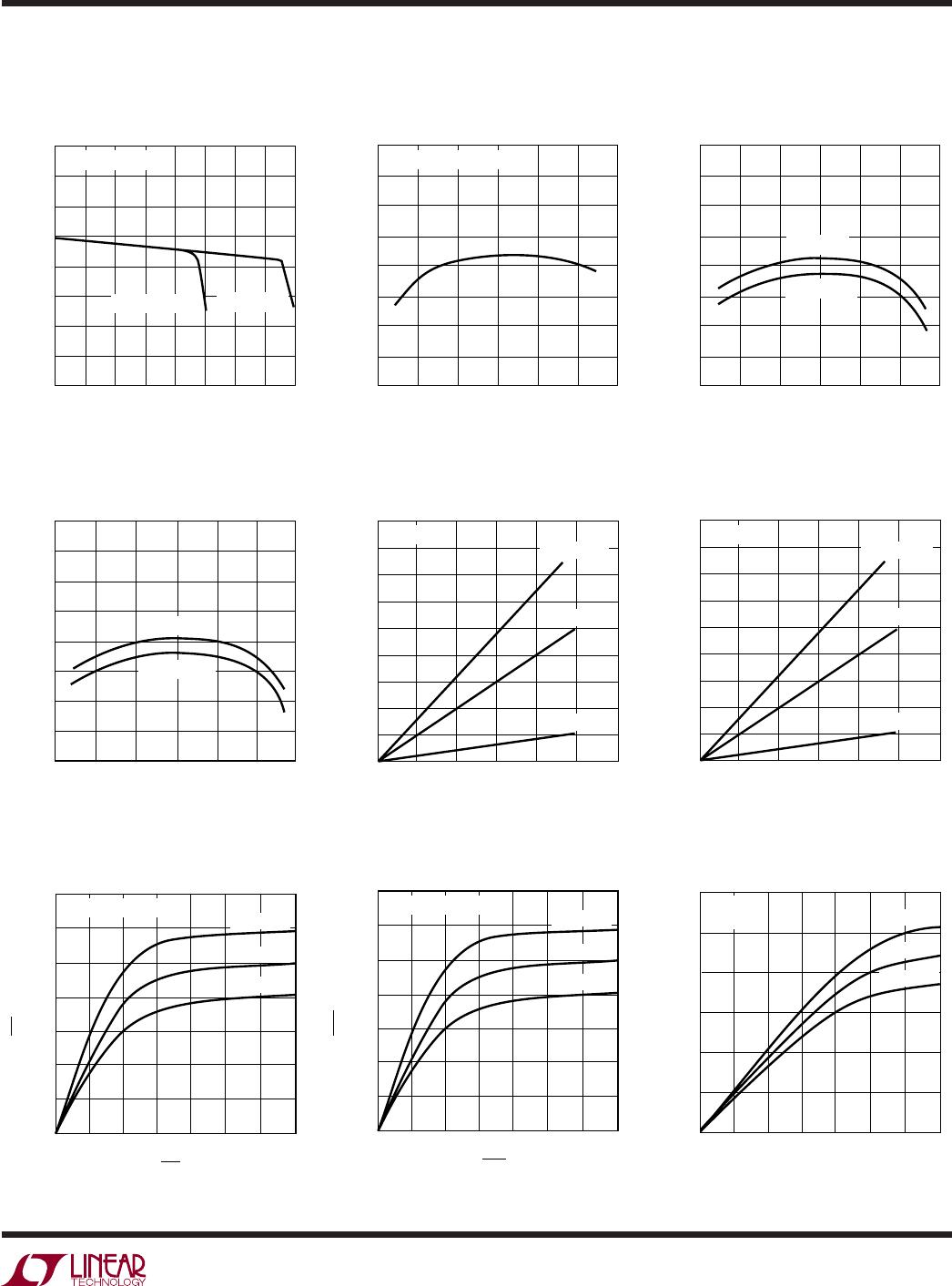
IUSB Pin Voltage vs Temperature
(Constant-Current Mode)
Charge Current vs IDC Pin Voltage
Charge Current
vs IUSB Pin Voltage
P
W
R Pin I-V Curve
C
H
R
G Pin I-V Curve USBPWR Pin I-V Curve
Regulated Charger Output (Float)
Voltage vs Charge Current
Regulated Charger Output (Float)
Voltage vs Temperature
IDC Pin Voltage vs Temperature
(Constant-Current Mode)
TYPICAL PERFOR A CE CHARACTERISTICS
UW
T
A
= 25°C, unless otherwise noted.
LTC3550-1
6
35501f
I
BAT
(mA)
1000
800
600
400
200
0
3550-1 G10
TEMPERATURE (°C)
–50 25 75
–25 0
50 100 125
V
DCIN
= V
USBIN
= 5V
V
BAT
= 4V
θ
JA
= 40°C/W
R
IDC
= 1.25k
R
IDC
= R
IUSB
= 2k
ONSET OF
THERMAL REGULATION
V
DCIN
(V)
I
BAT
(mA)
3550-1 G11
900
800
700
600
500
400
300
4.0
5.0
6.0
6.5
4.5 5.5
7.0
7.5
8.0
R
IDC
= 1.25k
V
BAT
= 4V
θ
JA
= 35°C/W
ONSET OF
THERMAL REGULATION
V
BAT
(V)
2.4
I
BAT
(mA)
1000
800
600
400
200
0
3.0
3.6
3.9
3550-1 G12
2.7
3.3
4.2
4.5
V
DCIN
= V
USBIN
= 5V
θ
JA
= 40°C/W
R
IDC
= 1.25k
TEMPERATURE (°C)
–50
R
DS(ON)
(m)
550
500
450
400
350
300
250
25 75
3550-1 G13
–25 0
50 100 125
V
BAT
= 4V
I
BAT
= 200mA
TEMPERATURE (°C)
–50 25 75
–25 0
50 100 125
R
DS(ON)
(m)
800
750
700
650
600
550
500
450
400
350
3550-1 G14
V
BAT
= 4V
I
BAT
= 200mA
TEMPERATURE (°C)
–50 25 75
–25 0
50 100
V
ENABLE
(mV)
900
850
800
750
700
650
600
3550-1 G15
V
DCIN
= V
USBIN
= 5V
TEMPERATURE (°C)
–50 25 75
–25 0
50 100
I
DCIN
(µA)
3550-1 G16
50
45
40
35
30
25
20
15
10
5
0
V
DCIN
= 8V
V
DCIN
= 5V
V
DCIN
= 4.3V
ENABLE = 5V
TEMPERATURE (°C)
–50 25 75
–25 0
50 100
I
USBIN
(µA)
45
40
35
30
25
20
15
10
5
0
3550-1 G17
V
USBIN
= 8V
V
USBIN
= 5V
V
USBIN
= 4.3V
ENABLE = 0V
TEMPERATURE (°C)
–50 25 75
–25 0
50 100
3550-1 G18
R
ENABLE
(M)
2.8
2.6
2.4
2.2
2.0
1.8
1.6
Charge Current
vs Ambient Temperature
Charge Current
vs Supply Voltage
Charge Current vs Battery Voltage
DCIN Power FET On-Resistance
vs Temperature
USBIN Power On-Resistance
vs Temperature
ENABLE Pin Threshold Voltage
(On-to-Off) vs Temperature
DCIN Shutdown Current
vs Temperature
USBIN Shutdown Current
vs Temperature
ENABLE Pin Pulldown Resistance
vs Temperature
TYPICAL PERFOR A CE CHARACTERISTICS
UW
T
A
= 25°C, unless otherwise noted.

LTC3550EDHC-1#PBF

Mfr. #:
Manufacturer:
Analog Devices / Linear Technology
Description:
Battery Management Dual Input USB/AC Adapter Li-Ion Battery Charger w/ 600mA Buck Converter
Lifecycle:
New from this manufacturer.
Delivery:
DHL FedEx Ups TNT EMS
Payment:
T/T Paypal Visa MoneyGram Western Union

Products related to this Datasheet