LTC3550-1
19
35501f
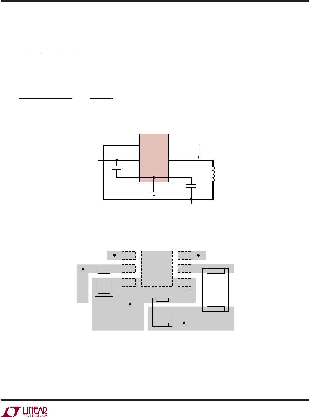
APPLICATIO S I FOR ATIO
WUU
U
However, the user may wish to repeat the previous analysis
to take the buck regulator’s power dissipation into account.
Equation (6) can be modifi ed to take into account the
temperature rise due to the buck regulator:
I
CT P
VV
BAT
A D BUCK JA
IN BAT JA
=
°−105 – ( • )
(– •
()
)
θ
θ
(7)
For optimum performance, it is critical that the exposed
metal pad on the backside of the LTC3550-1 package is
properly soldered to the PC board ground. When correctly
soldered to a 2500mm
2
double sided 1oz copper board,
the LTC3550-1 has a thermal resistance of approximately
40°C/W. Failure to make thermal contact between the ex-
posed pad on the backside of the package and the copper
board will result in thermal resistances far greater than
40°C/W. As an example, a correctly soldered LTC3550-1
can deliver over 800mA to a battery from a 5V supply
at room temperature. Without a good backside thermal
connection, this number would drop to much less than
500mA.
Battery Charger Stability Considerations
The constant-voltage mode feedback loop is stable without
any compensation provided a battery is connected to the
charger output. When the charger is in constant-current
mode, the charge current program pin (IDC or IUSB) is in
the feedback loop, not the battery. The constant-current
mode stability is affected by the impedance at the charge
current program pin. With no additional capacitance on
this pin, the charger is stable with program resistor val-
ues as high as 20k (I
CHG
= 50mA); however, additional
capacitance on these nodes reduces the maximum allowed
program resistor value.
Checking Regulator Transient Response
The regulator loop response can be checked by looking
at the load transient response. Switching regulators take
several cycles to respond to a step in load current. When
a load step occurs, V
OUT
immediately shifts by an amount
equal to (ΔI
LOAD
• ESR), where ESR is the effective series
resistance of C
OUT
. ΔI
LOAD
also begins to charge or dis-
charge C
OUT
, which generates a feedback error signal. The
regulator loop then acts to return V
OUT
to its steady state
value. During this recovery time V
OUT
can be monitored
for overshoot or ringing that would indicate a stability
problem. For a detailed explanation of switching control
loop theory, see Application Note 76.
A second, more severe transient is caused by switching
in loads with large (>1µF) supply bypass capacitors. The
discharged bypass capacitors are effectively put in paral-
lel with C
OUT
, causing a rapid drop in V
OUT
. No regulator
can deliver enough current to prevent this problem if the
load switch resistance is low and it is driven quickly. The
only solution is to limit the rise time of the switch drive
so that the load rise time is limited to approximately (25
• C
LOAD
). Thus, a 10µF capacitor charging to 3.3V would
require a 250µs rise time, limiting the charging current
to about 130mA.
Protecting the USB Pin and Wall Adapter Input from
Overvoltage Transients
Caution must be exercised when using ceramic capaci-
tors to bypass the USBIN pin or the wall adapter inputs.
High voltage transients can be generated when the USB
or wall adapter is hot-plugged. When power is supplied
via the USB bus or wall adapter, the cable inductance
along with the self resonant and high Q characteristics of
ceramic capacitors can cause substantial ringing which
could exceed the maximum voltage ratings and damage
the LTC3550-1. Refer to Linear Technology Application
Note 88, entitled “Ceramic Input Capacitors Can Cause
Overvoltage Transients” for a detailed discussion of this
problem. The long cable lengths of most wall adapters
and USB cables makes them especially susceptible to this
problem. To bypass the USB and the wall adapter inputs,
add a 1Ω resistor in series with a ceramic capacitor to
lower the effective Q of the network and greatly reduce the
ringing. A tantalum, OS-CON, or electrolytic capacitor can
be used in place of the ceramic and resistor, as their higher
ESR reduces the Q, thus reducing the voltage ringing.
The oscilloscope photograph in Figure 4 shows how seri-
ous the overvoltage transient can be for the USB and wall
adapter inputs. For both traces, a 5V supply is hot-plugged
using a three foot long cable. For the top trace, only a
4.7µF ceramic X5R capacitor (without the recommended
1Ω series resistor) is used to locally bypass the input.
This trace shows excessive ringing when the 5V cable
is inserted, with the overvoltage spike reaching 10V. For