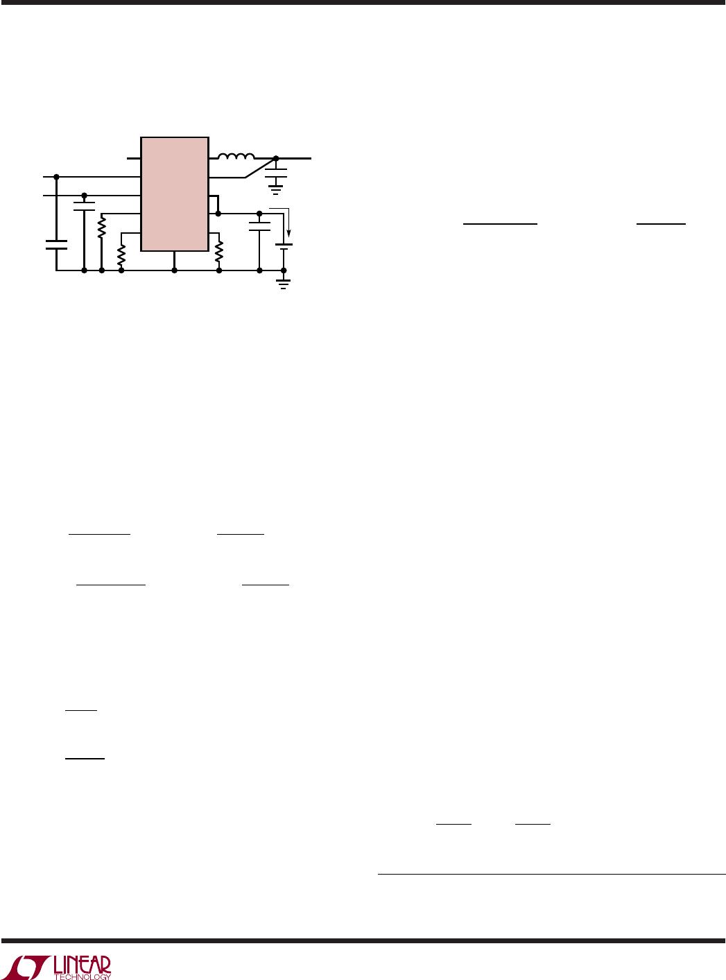
LTC3550-1
13
35501f
OPERATIO
U
600mA Step-Down Regulator
The LTC3550-1 regulator uses a constant frequency, cur-
rent mode step-down architecture. Both the top (P-channel
MOSFET) and bottom (N-channel MOSFET) switches are
internal. During normal operation, the internal top power
MOSFET is turned on each cycle when the oscillator sets
the RS latch, and is turned off when the current com-
parator, I
COMP
, resets the RS latch. The peak inductor
current at which I
COMP
resets the RS latch, is controlled
by the output of error amplifi er EA. When the load current
increases, it causes a slight decrease in the output voltage
(V
OUT
), relative to the internal reference, which in turn
causes the EA amplifi er’s output voltage to increase until
the average inductor current matches the new load cur-
rent. While the top MOSFET is off, the bottom MOSFET is
turned on until either the inductor current starts to reverse,
as indicated by the current reversal comparator I
RCMP
, or
the beginning of the next clock cycle.
Burst Mode
®
Operation
The LTC3550-1 buck regulator is capable of Burst Mode
operation in which the internal power MOSFETs operate
intermittently based on load current demand.
In Burst Mode operation, the peak current of the inductor is
set to approximately 200mA regardless of the output load.
Each burst event can last from a few cycles at light loads
to almost continuously cycling with short sleep intervals
at moderate loads. In between these burst events, the
power MOSFETs and any unneeded circuitry are turned
off, reducing the quiescent current to 20µA. In this sleep
state, the load current is being supplied solely from the
output capacitor. As the output voltage droops, the EA
amplifi er’s output rises above the sleep threshold signaling
the BURST comparator to trip and turn the top MOSFET
on. This process repeats at a rate that is dependent on
the load demand.
Dropout Operation
As the input supply voltage decreases to a value approach-
ing the output voltage, the duty cycle increases toward the
maximum on-time. Further reduction of the supply voltage
forces the main switch to remain on for more than one cycle
until it reaches 100% duty cycle. The output voltage will
then be determined by the input voltage minus the voltage
drop across the P-channel MOSFET and the inductor.
An important detail to remember is that at low input supply
voltages, the R
DS(ON)
of the P-channel switch increases
(see Typical Performance Characteristics). Therefore,
the user should calculate the power dissipation when the
LTC3550-1 is used at 100% duty cycle with low input
voltage (See Thermal Considerations in the Applications
Information section).
Battery Charger Power Source Selection
The LTC3550-1 can charge a battery from either the wall
adapter input or the USB port input. The charger automati-
cally senses the presence of voltage at each input. If both
power sources are present, the charger defaults to the wall
adapter source provided suffi cient power is present at the
DCIN input. “Suffi cient power” is defi ned as:
• Supply voltage is greater than the UVLO threshold.
• Supply voltage is greater than the battery voltage by
50mV (180mV rising, 50mV falling).
The open drain power status outputs (
P
W
R and USBPWR)
indicate which power source has been selected. Table 1
describes the behavior of these status outputs.
Table 1. Power Source Selection
V
USBIN
> 3.95V and
V
USBIN
> BAT + 50mV
V
USBIN
< 3.95V or
V
USBIN
< BAT + 50mV
V
DCIN
> 4.15V and
V
DCIN
> BAT + 50mV
Device Powered from
Wall Adapter Source;
USBIN Current < 25µA
P
W
R: LOW
USBPWR: LOW
Device Powered from
Wall Adapter Source
P
W
R: LOW
USBPWR: LOW
V
DCIN
< 4.15V or
V
DCIN
< BAT + 50mV
Device Powered from
USB Source;
P
W
R: LOW
USBPWR: Hi-Z
No Charging
P
W
R: Hi-Z
USBPWR: LOW
Status Indicators
The charge status output (
C
H
R
G) has two states: pull-
down and high impedance. The pull-down state indicates
that the LTC3550-1 is in a charge cycle. Once the charge
cycle has terminated or the LTC3550-1 is disabled, the
pin state becomes high impedance. The pull-down state
is strong enough to drive an LED and is capable of sink-
ing up to 10mA.
Burst Mode is a registered trademark of Linear Technology Corporation.
LTC3550-1
14
35501f
OPERATIO
U
The power supply status output (
P
W
R) has two states: pull-
down and high impedance. The pull-down state indicates
that power is present at either DCIN or USBIN. If no power
is applied at either pin, the
P
W
R pin is high impedance,
indicating that the LTC3550-1 lacks suffi cient power to
charge the battery. The pull-down state is strong enough
to drive an LED and is capable of sinking up to 10mA.
The USB power status output (USBPWR) has two states:
pull-down and high impedance. The high impedance state
indicates that the LTC3550-1 is being powered from the
USBIN input. The pull-down state indicates that the charger
is either powered from DCIN or is in a UVLO condition
(see Table 1). The pull-down state is capable of sinking
up to 1mA.
Thermal Limiting
An internal thermal feedback loop reduces the programmed
charge current if the die temperature attempts to rise
above a preset value of approximately 105°C. This feature
protects the LTC3550-1 from excessive temperature and
allows the user to push the limits of the power handling
capability of a given circuit board without risk of damag-
ing the device. The charge current can be set according
to typical (not worst-case) ambient temperature with the
assurance that the charger will automatically reduce the
current in worst case conditions. DFN package power
considerations are discussed further in the Applications
Information section.
Charge Current Soft-Start and Soft-Stop
The battery charger includes a soft-start circuit to minimize
the inrush current at the start of a charge cycle. When a
charge cycle is initiated, the charge current ramps from
zero to full-scale current over a period of 250µs. Like-
wise, internal circuitry slowly ramps the charge current
from full-scale to zero in approximately 30µs when the
charger shuts down or self terminates. This minimizes
the transient current load on the power supply during
start-up and shut-off.
Short-Circuit Protection
When the regulator output (V
OUT
) is shorted to ground, the
frequency of the oscillator is reduced to about 210kHz, one
seventh the nominal frequency. This frequency foldback
ensures that the inductor current has more time to decay,
thereby preventing runaway. The oscillator’s frequency
will progressively increase to 1.5MHz when V
OUT
rises
above 0V.
LTC3550-1
15
35501f
APPLICATIO S I FOR ATIO
WUU
U
Figure 2 shows the basic LTC3550-1 application circuit.
External component selection is driven by the charging
requirements and the buck regulator load requirements.
Programming Charge Termination
The charge cycle terminates when the charge current falls
below the programmed termination threshold during con-
stant-voltage mode. This threshold is set by connecting an
external resistor, R
ITERM
, from the ITERM pin to ground.
The charge termination current threshold (I
TERMINATE
) is
set by the following equation:
R
V
I
I
V
R
ITERM
TERMINATE
TERMINATE
ITERM
==
100 100
,
The termination condition is detected by using an internal
ltered comparator to monitor the ITERM pin. When the
ITERM pin voltage drops below 100mV* for longer than
t
TERMINATE
(typically 1.5ms), charging is terminated. The
charge current is latched off and the LTC3550-1 enters
standby mode.
When charging, transient loads on the BAT pin can cause
the ITERM pin to fall below 100mV for short periods of
time before the DC charge current has dropped below the
programmed termination current. The 1.5ms fi lter time
(t
TERMINATE
) on the termination comparator ensures that
transient loads of this nature do not result in premature
charge cycle termination. Once the average charge current
drops below the programmed termination threshold, the
LTC3550-1 terminates the charge cycle and stops providing
any current out of the BAT pin. In this state, any load on
the BAT pin must be supplied by the battery.
Buck Regulator Inductor Selection
For most applications, the value of the inductor will fall in
the range of 1µH to 4.7µH. Its value is chosen based on
the desired inductor ripple current. Large value inductors
lower ripple current and small value inductors result in
higher ripple currents. Higher V
CC
or V
OUT
also increases
the ripple current as shown in Equation 1. A reasonable
starting point for setting ripple current is ΔI
L
= 240mA
(40% of 600mA).
∆=
I
V
fL
V
V
L
OUT
O
OUT
CC
•1
(1)
Programming and Monitoring Charge Current
The charge current delivered to the battery from the wall
adapter supply is programmed using a single resistor
from the IDC
pin to ground. Likewise, the charge current
from the USB supply is programmed using a single resis-
tor from the IUSB pin to ground. The program resistor
and the charge current (I
CHRG
) are calculated using the
following equations:
R
V
I
I
V
R
R
IDC
CHRG DC
CHRG DC
IDC
IUS
==
1000 1000
()
()
,
BB
CHRG USB
CHRG USB
IUSB
V
I
I
V
R
==
1000 1000
()
()
,
Charge current out of the BAT pin can be determined at
any time by monitoring the IDC or IUSB pin voltage and
using the following equations:
I
V
R
ch ing from wall adapter
BAT
IDC
IDC
= •(arg )1000
II
V
R
ch ing from USB ply
BAT
IUSB
IUSB
= •(arg sup1000 ))
Figure 2. LTC3550-1 Basic Circuit
* Any external sources that hold the ITERM pin above 100mV will prevent the LTC3550-1
from terminating a charge cycle.
R
IDC
R
IUSB
WALL
ADAPTER
USB
POWER
C2
C1
3550-1 F02
LTC3550-1
RUN
DCIN
USBIN
IUSB
IDC
SW
V
OUT
V
CC
BAT
GND
C
OUT
ITERM
+
L1
4.2V
SINGLE
CELL Li-Ion
BATTERY
V
OUT
1.875V
600mA
R
ITERM
C
IN

LTC3550EDHC-1#PBF

Mfr. #:
Manufacturer:
Analog Devices / Linear Technology
Description:
Battery Management Dual Input USB/AC Adapter Li-Ion Battery Charger w/ 600mA Buck Converter
Lifecycle:
New from this manufacturer.
Delivery:
DHL FedEx Ups TNT EMS
Payment:
T/T Paypal Visa MoneyGram Western Union

Products related to this Datasheet