General Description
The MAX2120 low-cost, direct-conversion tuner IC is
designed for satellite set-top and VSAT applications.
The IC is intended for QPSK, Digital Video Broadcast
(DVB-S), DSS, and free-to-air applications.
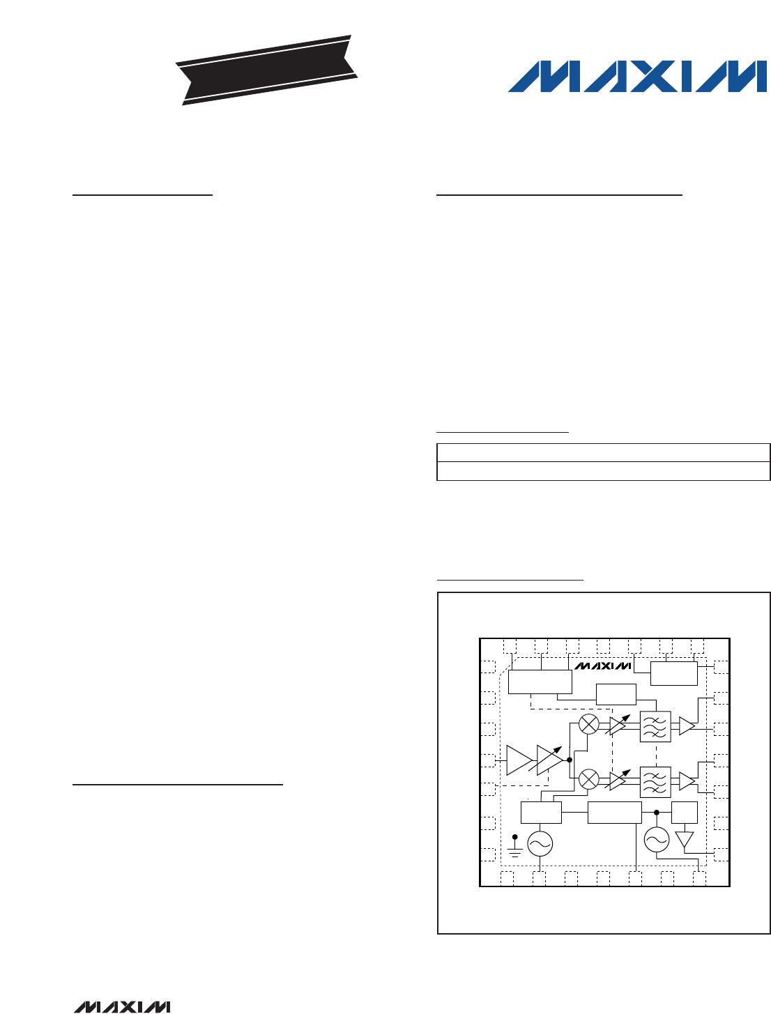
The MAX2120 directly converts the satellite signals
from the LNB to baseband using a broadband I/Q
downconverter. The operating frequency range extends
from 925MHz to 2175MHz.
The device includes an LNA and an RF variable-gain
amplifier, I and Q downconverting mixers, and baseband
lowpass filters with programmable cutoff frequency
control and digitally controlled baseband variable-gain
amplifiers. Together, the RF and baseband variable-gain
amplifiers provide more than 80dB of gain-control range.
The IC is compatible with virtually all QPSK demodulators.
The MAX2120 includes fully monolithic VCOs, as well as
a complete frequency synthesizer. Additionally, an on-
chip crystal oscillator is provided along with a buffered
output for driving additional tuners and demodulators.
Synthesizer programming and device configuration are
accomplished with a 2-wire serial interface. The IC fea-
tures a VCO autoselect (VAS) function that automatically
selects the proper VCO. For multituner applications, the
device can be configured to have one of two 2-wire
interface addresses. A low-power standby mode is
available whereupon the signal path is shut down while
leaving the reference oscillator, digital interface, and
buffer circuits active, providing a method to reduce
power in single and multituner applications.
The MAX2120 is the most advanced DBS tuner available
today. The low noise figure eliminates the need for an
external LNA. A small number of passive components are
needed to form a complete DVB, DBS, or VSAT RF front-
end solution. The tuner is available in a very small 28-pin
thin QFN package.
Applications
DirecTV and Dish Network DBS
DVB-S
Two-Way Satellite Systems
VSATs
Free-to-Air
Features
o 925MHz to 2175MHz Frequency Range
o Monolithic VCO: No Calibration Required
o -75dBm to 0dBm High Dynamic Range
o 4MHz to 40MHz Integrated Variable BW LP Filters
o Single +3.3V ±5% Supply
o Low-Power Standby Mode
o Address Pin for Multituner Applications
o Differential I/Q Interface
o I
2
C 2-Wire Serial Interface
o Very Small 28-Pin Thin QFN Package
MAX2120
Complete, Direct-Conversion Tuner for DVB-S
and Free-to-Air Applications
________________________________________________________________
Maxim Integrated Products
1
19-0832; Rev 2; 5/10
For pricing, delivery, and ordering information, please contact Maxim Direct at 1-888-629-4642,
or visit Maxim’s website at www.maxim-ic.com.
EVALUATION KIT
AVAILABLE
VTUNE
GNDSYN
CPOUT
VCC_SYN
XTAL
VCOBYP
SCL
VCC_BB
QDC-
ADDR
QDC+
IDC-
RFIN
GC1
VCC_LO
+
÷
IOUT+
QOUT-
VCC_DIG
GNDTUNE
SDA
19
17
16
3
5
18
4
6
VCC_VCO
REFOUT
15
7
GND
IOUT-
20
2
VCC_RF1
21
IDC+
1
26 24 23
10 12
25
11 13
22
14
27
9
28
8
VCC_RF2
MAX2120
INTERFACE LOGIC
AND CONTROL
DC OFFSET
CORRECTION
LPF BW
CONTROL
DIV2/DIV4
EP
FREQUENCY
SYNTHESIZER
QOUT+
Pin Configuration/
Functional Diagram
Ordering Information
PART TEMP RANGE PIN-PACKAGE
MAX2120CTI+ 0°C to +70°C 28 Thin QFN-EP*
*
EP = Exposed paddle.
+
Denotes a lead(Pb)-free/RoHS-compliant package.
MAX2120
Complete, Direct-Conversion Tuner for DVB-S
and Free-to-Air Applications
2 _______________________________________________________________________________________
ABSOLUTE MAXIMUM RATINGS
Stresses beyond those listed under “Absolute Maximum Ratings” may cause permanent damage to the device. These are stress ratings only, and functional
operation of the device at these or any other conditions beyond those indicated in the operational sections of the specifications is not implied. Exposure to
absolute maximum rating conditions for extended periods may affect device reliability.
V
CC
to GND...........................................................-0.3V to +3.9V
All Other Pins to GND.................................-0.3V to (V
CC
+ 0.3V)
RF Input Power: RFIN .....................................................+10dBm
VCOBYP, CPOUT, REFOUT, XTAL, IOUT_, QOUT_, IDC_, and
QDC_ Short-Circuit Protection.............................................10s
Continuous Power Dissipation (T
A
= +70°C)
28-Pin Thin QFN (derated 34.5mW/°C above +70°C)........2.75W
Operating Temperature Range...............................0°C to +70°C
Junction Temperature......................................................+150°C
Storage Temperature Range .............................-65°C to +160°C
Lead Temperature (soldering, 10s) .................................+300°C
Soldering Temperature (reflow) .......................................+260°C
DC ELECTRICAL CHARACTERISTICS
(MAX2120 Evaluation Kit: V
CC
= +3.13V to +3.47V, V
GC1
= +0.5V (max gain), T
A
= 0°C to +70°C. No input signals at RF, baseband
I/Os are open circuited, and LO frequency = 2150MHz. Default register settings except BBG[3:0] = 1011. Typical values measured
at V
CC
= +3.3V, T
A
= +25°C, unless otherwise noted.) (Note 1)
PARAMETER CONDITIONS MIN TYP MAX UNITS
SUPPLY
Supply Voltage 3.13 3.3 3.47 V
Receive mode, bit STBY = 0 100 160
Supply Current
Standby mode, bit STBY = 1 3
mA
ADDRESS SELECT INPUT (ADDR)
Digital Input-Voltage High, V
IH
2.4 V
Digital Input-Voltage Low, V
IL
0.5 V
Digital Input-Current High, I
IH
50 µA
Digital Input-Current Low, I
IL
-50 µA
ANALOG GAIN-CONTROL INPUT (GC1)
Input Voltage Range Maximum gain = 0.5V 0.5 2.7 V
Input Bias Current -50 +50 µA
VCO TUNING VOLTAGE INPUT (VTUNE)
Input Voltage Range 0.4 2.3 V
2-WIRE SERIAL INPUTS (SCL, SDA)
Clock Frequency 400 kHz
Input Logic-Level High
0.7 x
V
CC
V
Input Logic-Level Low
0.3 x
V
CC
V
Input Leakage Current Digital inputs = GND or V
CC
±0.1 ±1 µA
2-WIRE SERIAL OUTPUT (SDA)
Output Logic-Level Low I
SINK
= 1mA 0.4 V
CAUTION! ESD SENSITIVE DEVICE
MAX2120
Complete, Direct-Conversion Tuner for DVB-S
and Free-to-Air Applications
_______________________________________________________________________________________ 3
AC ELECTRICAL CHARACTERISTICS
(MAX2120 Evaluation Kit: V
CC
= +3.13V to +3.47V, V
GC1
= +0.5V (max gain), T
A
= 0°C to +70°C. Default register settings except
BBG[3:0] = 1011. Typical values measured at V
CC
= +3.3V, T
A
= +25°C, unless otherwise noted.) (Note 1)
PARAMETER CONDITIONS MIN TYP MAX UNITS
MAIN SIGNAL PATH PERFORMANCE
Input Frequency Range (Note 2) 925 2175 MHz
RF Gain-Control Range (GC1) 0.5V < V
GC1
< 2.7V 65 73 dB
Baseband Gain-Control Range Bits GC2 = 1111 to 0000 13 15 dB
In-Band Input IP3 (Note 3) +2 dBm
Out-of-Band Input IP3 (Note 4) +15 dBm
Input IP2 (Note 5) +40 dBm
Adjacent Channel Protection (Note 6) 25 dB
V
GC1
is set to 0.5V (maximum RF gain) and BBG[3:0] is
adjusted to give a 1V
P-P
baseband output level for a
-75dBm CW input tone at 1500MHz
8
Noise Figure
Starting with the same BBG[3:0] setting as above, V
GC1
is adjusted to back off RF gain by 10dB (Note 7)
912
dB
Minimum RF Input Return Loss 925MHz < f
RF
< 2175MHz, in 75 system 12 dB
BASEBAND OUTPUT CHARACTERISTICS
Nominal Output Voltage Swing R
LOAD
= 2k//10pF 0.5 1 V
P-P
I/Q Amplitude Imbalance Measured at 500kHz; filter set to 22.27MHz ±1 dB
I/Q Quadrature Phase Imbalance Measured at 500kHz; filter set to 22.27MHz 3.5 Degrees
Single-Ended I/Q Output
Impedance
Real Z
O
, from 1MHz to 40MHz 30
Output 1dB Compression Voltage Differential 3 V
P-P
Baseband Highpass -3dB
Frequency Corner
47nF capacitors at IDC_, QDC_ 400 Hz
BASEBAND LOWPASS FILTERS
Filter Bandwidth Range 4 40 MHz
Rejection Ratio At 2 x f
-3dB
39 dB
Group Delay Up to 1dB bandwidth 37 ns
Ratio of In-Filter-Band to Out-of-
Filter-Band Noise
f
INBAND
= 100Hz to 22.5MHz, f
OUTBAND
= 87.5MHz to
112.5MHz
25 dB
FREQUENCY SYNTHESIZER
RF-Divider Frequency Range 925 2175 MHz
RF-Divider Range (N) 16 2175
Reference-Divider Frequency
Range
4 30 MHz
Reference-Divider Range (R) 1 31
Phase-Detector Comparison
Frequency
1 2 MHz

MAX2120CTI+

Mfr. #:
Manufacturer:
Maxim Integrated
Description:
Tuners Direct Conversion Tu Ner For Dvb-S -75 To
Lifecycle:
New from this manufacturer.
Delivery:
DHL FedEx Ups TNT EMS
Payment:
T/T Paypal Visa MoneyGram Western Union

Products related to this Datasheet