MAX2120
Complete, Direct-Conversion Tuner for DVB-S
and Free-to-Air Applications
______________________________________________________________________________________ 15
2-Wire Serial Interface
The MAX2120 uses a 2-wire I
2
C-compatible serial
interface consisting of a serial data line (SDA) and a
serial clock line (SCL). SDA and SCL facilitate bidirec-
tional communication between the MAX2120 and the
master at clock frequencies up to 400kHz. The master
initiates a data transfer on the bus and generates the
SCL signal to permit data transfer. The MAX2120
behaves as a slave device that transfers and receives
data to and from the master. SDA and SCL must be
pulled high with external pullup resistors (1kΩ or
greater) for proper bus operation.
One bit is transferred during each SCL clock cycle. A
minimum of nine clock cycles is required to transfer a
byte in or out of the MAX2120 (8 bits and an
ACK/NACK). The data on SDA must remain stable
during the high period of the SCL clock pulse. Changes
in SDA while SCL is high and stable are considered
control signals (see the
START and STOP Conditions
section). Both SDA and SCL remain high when the bus
is not busy. Pullup resistors should be referenced to the
MAX2120’s V
CC
.
START and STOP Conditions
The master initiates a transmission with a START condi-
tion (S), which is a high-to-low transition on SDA while
SCL is high. The master terminates a transmission with
a STOP condition (P), which is a low-to-high transition
on SDA while SCL is high.
Acknowledge and Not-Acknowledge Conditions
Data transfers are framed with an acknowledge bit
(ACK) or a not-acknowledge bit (NACK). Both the mas-
ter and the MAX2120 (slave) generate acknowledge
bits. To generate an acknowledge, the receiving device
must pull SDA low before the rising edge of the
acknowledge-related clock pulse (ninth pulse) and
keep it low during the high period of the clock pulse.
To generate a not-acknowledge condition, the receiver
allows SDA to be pulled high before the rising edge of
the acknowledge-related clock pulse, and leaves SDA
high during the high period of the clock pulse.
Monitoring the acknowledge bits allows for detection of
unsuccessful data transfers. An unsuccessful data
transfer happens if a receiving device is busy or if a
system fault has occurred. In the event of an unsuc-
cessful data transfer, the bus master must reattempt
communication at a later time.
Slave Address
The MAX2120 has a 7-bit slave address that must be
sent to the device following a START condition to initi-
ate communication. The slave address is internally pro-
grammed to 1100000. The eighth bit (R/W) following
the 7-bit address determines whether a read or write
operation will occur.
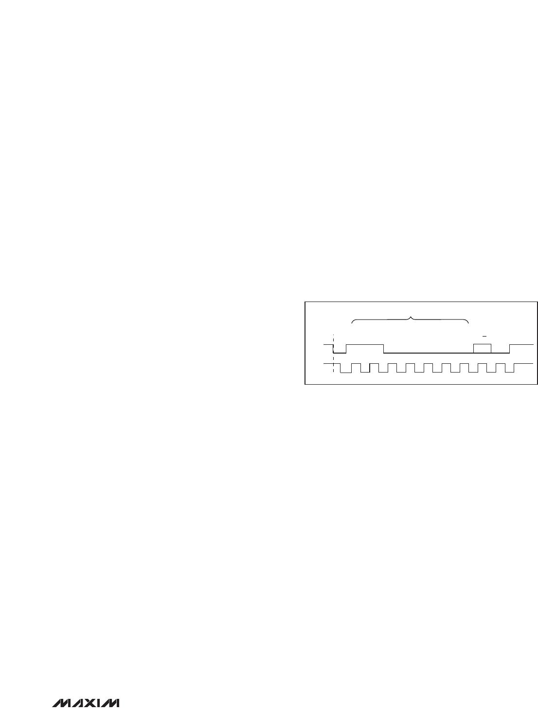
The MAX2120 continuously awaits a START condition
followed by its slave address. When the device recog-
nizes its slave address, it acknowledges by pulling the
SDA line low for one clock period; it is ready to accept
or send data depending on the R/W bit (Figure 1).
The write/read address is C0/C1 if the ADDR pin is con-
nected to ground. The write/read address is C2/C3 if
the ADDR pin is connected to V
CC
.
Write Cycle
When addressed with a write command, the MAX2120
allows the master to write to a single register or to multi-
ple successive registers.
A write cycle begins with the bus master issuing a
START condition followed by the seven slave address
bits and a write bit (R/W = 0). The MAX2120 issues an
ACK if the slave address byte is successfully received.
The bus master must then send to the slave the
address of the first register it wishes to write to (see
Table 1 for register addresses). If the slave acknowl-
edges the address, the master can then write one byte
to the register at the specified address. Data is written
beginning with the most significant bit. The MAX2120
again issues an ACK if the data is successfully written
to the register. The master can continue to write data to
the successive internal registers with the MAX2120
acknowledging each successful transfer, or it can ter-
minate transmission by issuing a STOP condition. The
write cycle will not terminate until the master issues a
STOP condition.