MAX2120
Complete, Direct-Conversion Tuner for DVB-S
and Free-to-Air Applications
12 ______________________________________________________________________________________
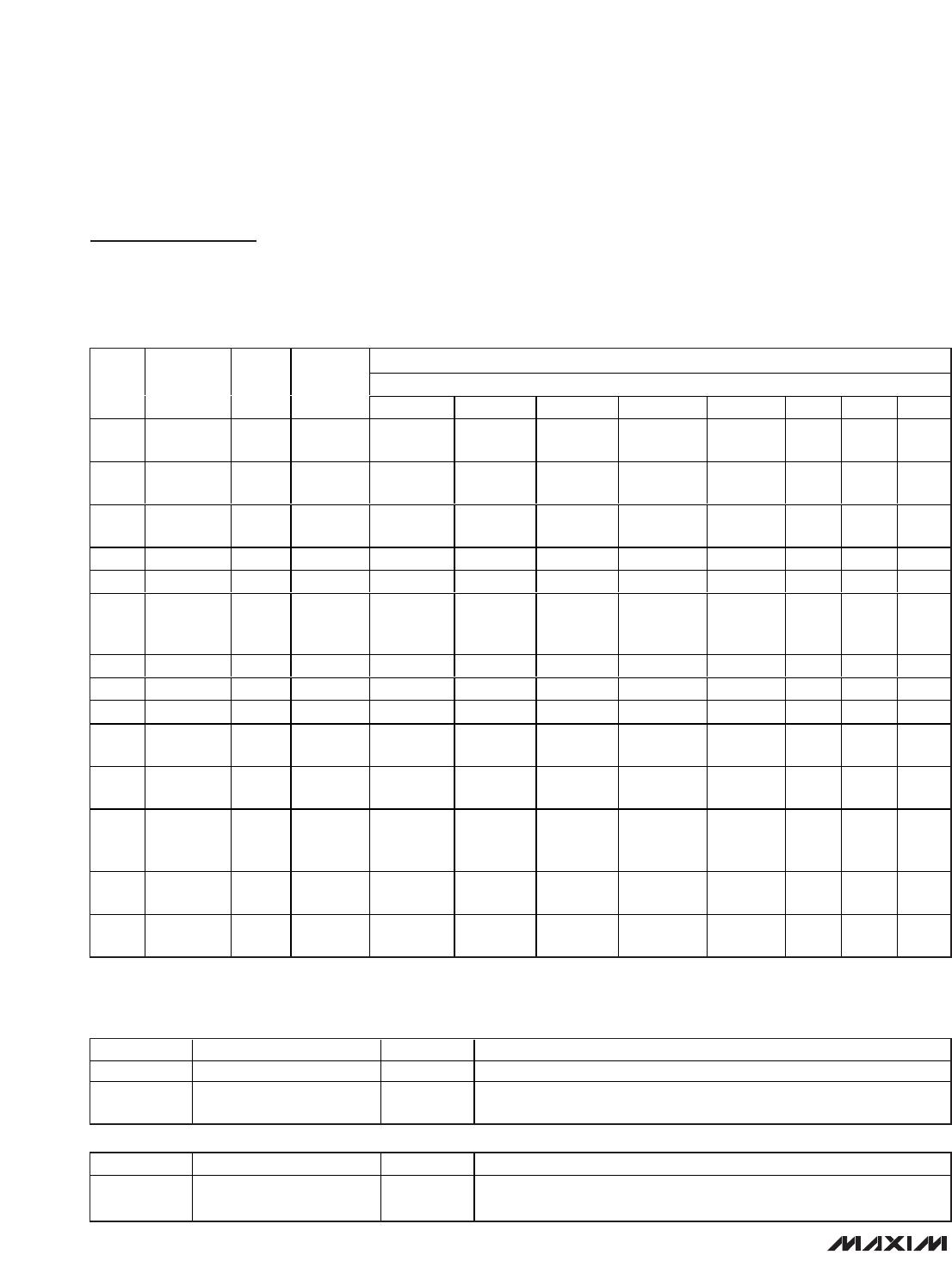
BIT NAME BIT LOCATION (0 = LSB) DEFAULT FUNCTION
VCO[4:0] 7–3 11001
Controls which VCO is activated when using manual VCO
programming mode. This also serves as the starting point for
the VCO autoselect mode.
VAS 2 1
VCO Autoselection (VAS) Circuit
0 = Disable VCO selection must be program through I
2
C
1 = Enable VCO selection controlled by autoselection circuit
ADL 1 0
Enables or disables the VCO tuning voltage ADC latch when
the VCO autoselect mode (VAS) is disabled.
0 = Disables the ADC latch
1 = Latches the ADC value
ADE 0 0
Enables or disables VCO tuning voltage ADC read when the
VCO autoselect mode (VAS) is disabled.
0 = Disables ADC read
1 = Enables ADC read
BIT NAME BIT LOCATION (0 = LSB) DEFAULT FUNCTION
LPF[7:0] 7–0 01001011
Sets the baseband lowpass filter 3dB corner frequency. 3dB
corner frequency = 4MHz + (LPF[7:0] - 12) x 290kHz.
Table 8. Lowpass Filter Register
BIT NAME BIT LOCATION (0 = LSB) DEFAULT FUNCTION
STBY 7 0
Software standby control.
0 = Normal operation
1 = Disables the signal path and frequency synthesizer, leaving
only the 2-wire bus, crystal oscillator, XTALOUT buffer, and
XTALOUT buffer divider active
X 6 X Don’t care.
PWDN 5 0
Factory use only.
0 = Normal operation; other value is not tested.
X 4 X Don’t care.
BBG[3:0] 3–0 0000
Baseband gain setting (1dB typical per step).
0000 = Minimum gain (0dB)
…
1111 = Maximum gain (15dB typical)
Table 9. Control Register