MAX2120
Complete, Direct-Conversion Tuner for DVB-S
and Free-to-Air Applications
16 ______________________________________________________________________________________
Figure 2 illustrates an example in which registers 0
through 2 are written with 0x0E, 0xD8, and 0xE1,
respectively.
Read Cycle
When addressed with a read command, the MAX2120
allows the master to read back a single register, or mul-
tiple successive registers.
A read cycle begins with the bus master issuing a
START condition followed by the 7 slave address bits
and a write bit (R/W = 0). The MAX2120 issues an ACK if
the slave address byte is successfully received. The bus
master must then send the address of the first register it
wishes to read (see Table 1 for register addresses). The
slave acknowledges the address. Then, a START condi-
tion is issued by the master, followed by the 7 slave
address bits and a read bit (R/W = 1). The MAX2120
issues an ACK if the slave address byte is successfully
received. The MAX2120 starts sending data MSB first
with each SCL clock cycle. At the 9th clock cycle, the
master can issue an ACK and continue to read succes-
sive registers, or the master can terminate the transmis-
sion by issuing a NACK. The read cycle does not
terminate until the master issues a STOP condition.
Figure 3 illustrates an example in which registers 0
through 2 are read back.
WRITE
DEVICE
ADDRESS
R/W ACK
WRITE
REGISTER
ADDRESS
ACK
WRITE DATA
TO REGISTER
0x00
ACK
WRITE DATA
TO REGISTER
0x01
ACK
WRITE DATA
TO REGISTER
0x02
ACK
START
1100000 0 0x00 0x0E 0xD8 0x0E1
STOP
Figure 2. Example: Write Registers 0 through 2 with 0x0E, 0xD8, and 0xE1, respectively.
DEVICE
ADDRESS
R / W
1100000
REGISTER
ADDRESS
000000000
S
T
A
R
T
S
T
A
R
T
A
C
K
A
C
K
REG 02
DATA
xxxxxxxx
S
T
O
P
N
A
C
K
REG 00
DATA
xxxxxxxx
A
C
K
REG 01
DATA
xxxxxxxx
A
C
K
A
C
K
DEVICE
ADDRESS
R / W
1100000 1
Figure 3. Example: Receive data from read registers.
MAX2120
Complete, Direct-Conversion Tuner for DVB-S
and Free-to-Air Applications
______________________________________________________________________________________ 17
Applications Information
The MAX2120 downconverts RF signals in the 925MHz to
2175MHz range directly to the baseband I/Q signals. The
devices are targeted for digital DBS tuner applications.
RF Input
The RF input of the MAX2120 is internally matched to
75. Only a DC-blocking capacitor is needed. See the
Typical Operating Circuit
.
RF Gain Control
The MAX2120 features a variable-gain low-noise amplifi-
er providing 73dB of RF gain range. The voltage-control
(VGC) range is 0.5V (minimum attenuation) to 2.7V
(maximum attenuation).
Baseband Variable-Gain Amplifier
The receiver baseband variable-gain amplifiers provide
15dB of gain-control range programmable in 1dB
steps. The VGA gain can be serially programmed
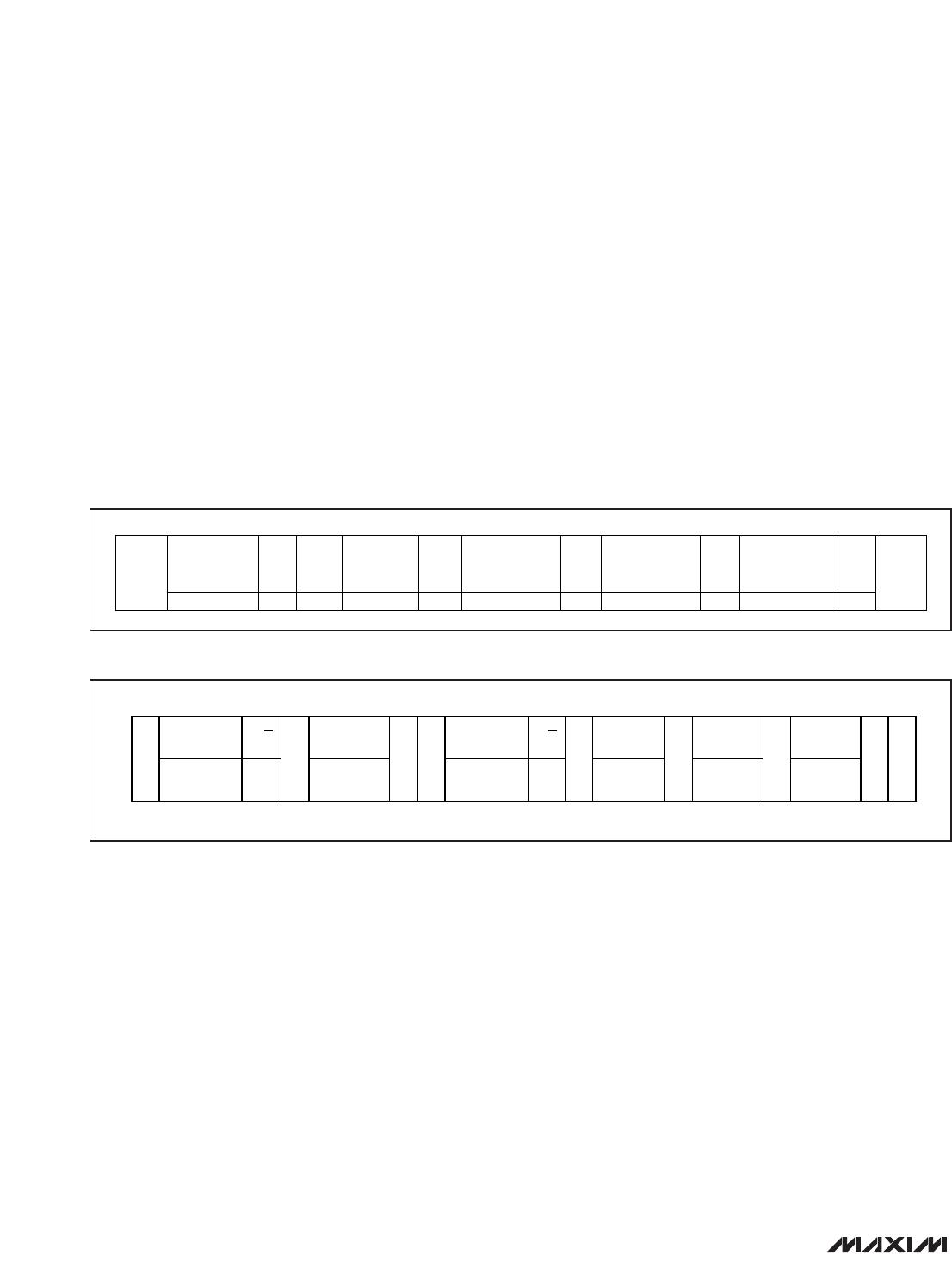
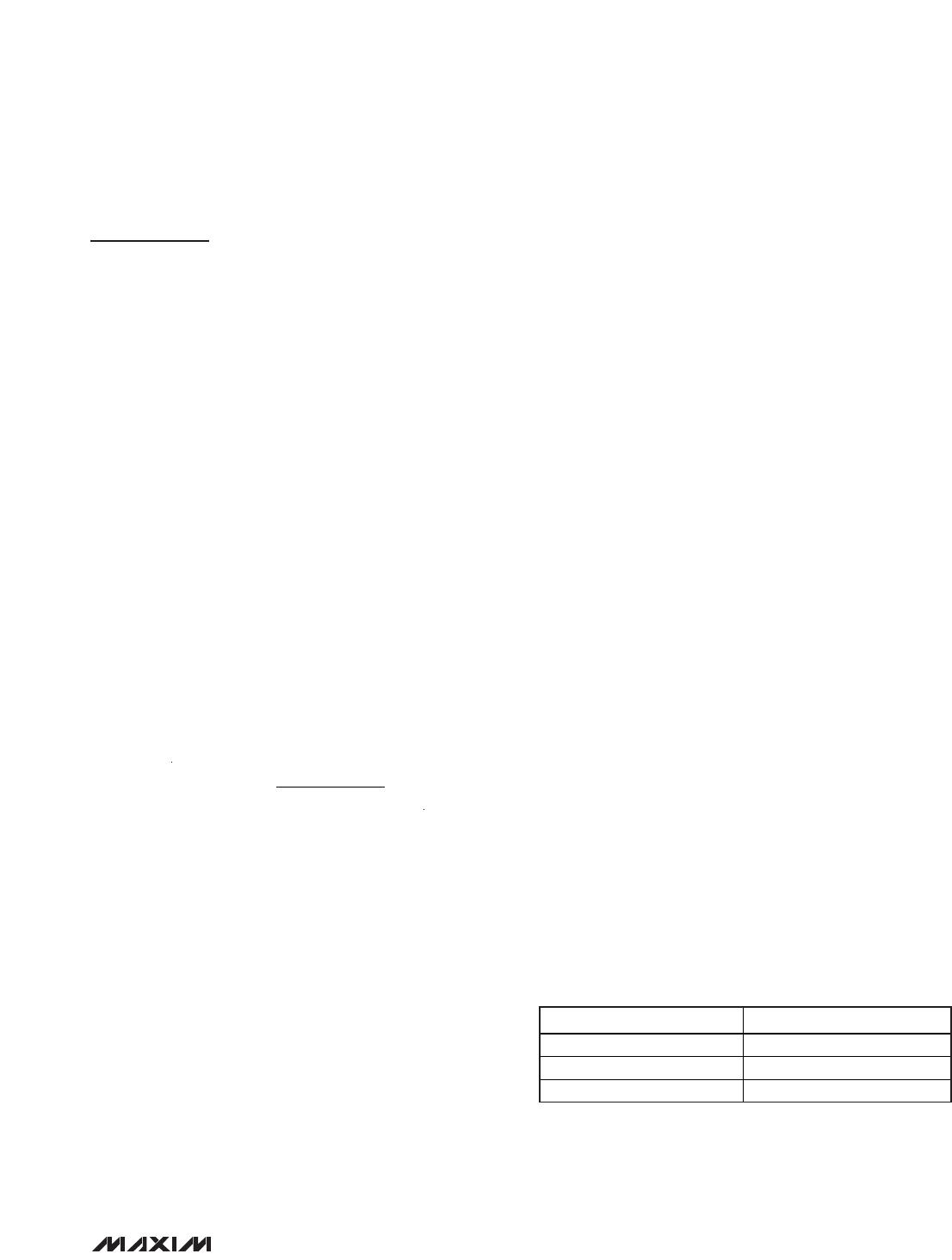
through the SPI™ interface by setting bits BBG[3:0] in
the Control register.
Baseband Lowpass Filter
The MAX2120 includes a programmable on-chip 7th-
order Butterworth filter. The -3dB corner frequency of
the baseband filter is programmable by setting the bits
LPF[7:0] in the Lowpass register. The value of the
LPF[7:0] is determined by the following equation:
where f
-3dB
is in units of MHz.
The filter can be adjusted from approximately 4MHz to
40MHz. Total device supply current depends on the fil-
ter BW setting, with increasing current commensurate
with increasing -3dB BW.
DC Offset Cancellation
The DC offset cancellation is required to maintain the I/Q
output dynamic range. Connecting an external capacitor
between IDC+ and IDC- forms a highpass filter for the I
channel, and an external capacitor between QDC+ and
QDC- forms a highpass filter for the Q channel. Keep the
value of the external capacitor less than 47nF to form a
typical highpass corner of 400Hz.
XTAL Oscillator
The MAX2120 contains an internal reference oscillator,
reference output divider, and output buffer. All that is
required is to connect a crystal through a series, 1nF
capacitor. To minimize parasitics, place the crystal and
series capacitor as close as possible to pin 14 (XTAL
pin). See Table 14 for crystal (XTAL) ESR (equivalent
series resistance) requirements. The typical input
capacitance is 40pF.
VCO Autoselect (VAS)
The MAX2120 includes 24 VCOs. The local oscillator fre-
quency can be manually selected by programming the
VCO[4:0] bits in the VCO register. The selected VCO is
reported in the Status Byte-2 register (see Table 13).
Alternatively, the MAX2120 can be set to autonomously
choose a VCO by setting the VAS bit in the VCO regis-
ter to logic-high. The VAS routine is initiated once the
N-divider LSB register word (REG 2) is loaded.
In the event that only the R-divider register or N-
divider MSB register word is changed, the N-divider
LSB word must also be loaded last to initiate the
VCO autoselect function. The VCO value pro-
grammed in the VCO[4:0] register serves as the start-
ing point for the automatic VCO selection process.
During the selection process, the VASE bit in the Status
Byte-1 register is cleared to indicate the autoselection
function is active. Upon successful completion, bits
VASE and VASA are set and the VCO selected is
reported in the Status Byte-2 register (see Table 13). If
the search is unsuccessful, VASA is cleared and VASE
is set. This indicates that searching has ended but no
good VCO has been found, and occurs when trying to
tune to a frequency outside the VCO’s specified
frequency range.
Refer to the MAX2112/MAX2120 VAS application note
for more information.
LPF[7:0]dec =
()
.
,
fMHz
MHz
dB
+
3
4
029
12
SPI is a trademark of Motorola, Inc.
ESR
MAX
() XTAL FREQUENCY (MHz)
150 4 < f
XTAL
6
100 6 < f
XTAL
8
40 8 < f
XTAL
13.5
Table 14. Maximum Cystal ESR
Requirements
MAX2120
Complete, Direct-Conversion Tuner for DVB-S
and Free-to-Air Applications
18 ______________________________________________________________________________________
3-Bit ADC
The MAX2120 has an internal 3-bit ADC connected to
the VCO tune pin (VTUNE). This ADC can be used for
checking the lock status of the VCOs.
Table 15 summarizes the ADC trip points, and the VCO
lock indication. The VCO autoselect routine will only
select a VCO in the “VAS locked” range. This allows
room for a VCO to drift over temperature and remain in
a valid “locked” range.
The ADC must first be enabled by setting the ADE bit in
the VCO register. The ADC reading is latched by a sub-
sequent programming of the ADC latch bit (ADL = 1).
The ADC value is reported in the Status Byte-2 register
(see Table 13).
Standby Mode
The MAX2120 features normal operating mode and
standby mode using the I
2
C interface. Setting a logic-
high to the PWDN bit in the Control register enables
power-down. In this mode, all circuitries except for the 2-
wire-compatible bus are disabled, allowing for program-
ming of the MAX2120 registers while in power-down.
In all cases, register settings loaded prior to entering
shutdown are saved upon transition back to active
mode. Default register values are provided for the
user’s convenience only. It’s the user’s responsibility to
load all the registers no sooner than 100µs after the
device is powered up.
Layout Considerations
The MAX2120 EV kit serves as a guide for PCB
layout. Keep RF signal lines as short as possible to mini-
mize losses and radiation. Use controlled impedance on
all high-frequency traces. For proper operation, the
exposed paddle must be soldered evenly to the board’s
ground plane. Use abundant vias beneath the exposed
paddle for maximum heat dissipation. Use abundant
ground vias between RF traces to minimize undesired
coupling. Bypass each V
CC
pin to ground with a 1nF
capacitor placed as close as possible to the pin.
ADC[2:0] LOCK STATUS
000 Out of Lock
001 Locked
010 VAS Locked
101 VAS Locked
110 Locked
111 Out of Lock
Table 15. ADC Trip Points and Lock Status

MAX2120CTI+

Mfr. #:
Manufacturer:
Maxim Integrated
Description:
Tuners Direct Conversion Tu Ner For Dvb-S -75 To
Lifecycle:
New from this manufacturer.
Delivery:
DHL FedEx Ups TNT EMS
Payment:
T/T Paypal Visa MoneyGram Western Union

Products related to this Datasheet