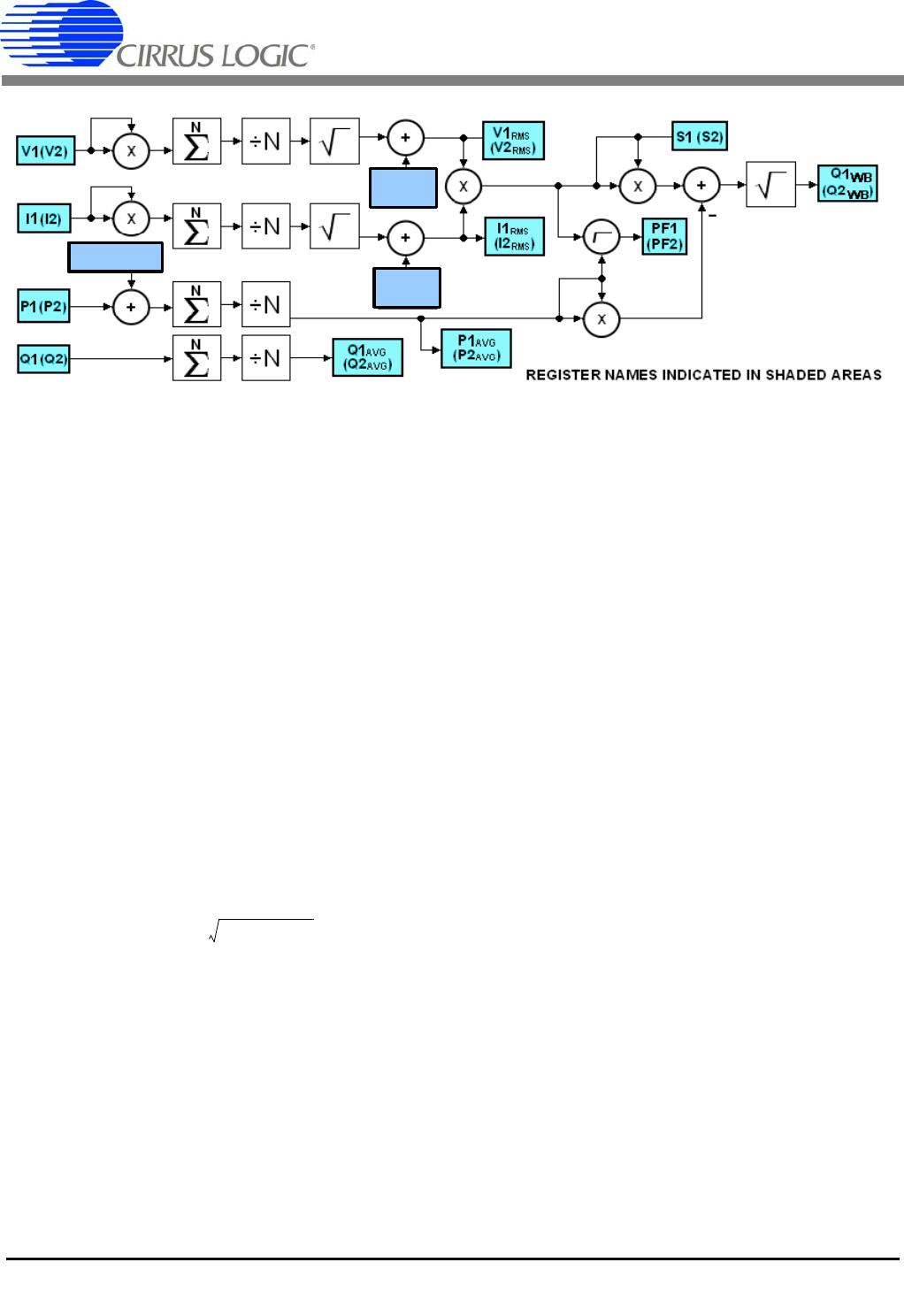
CS5464
16 DS682F3
4.8 Power and Energy Results
The instantaneous voltage and current samples are
multiplied to obtain the instantaneous power (
P1, P2)
(see Figure 3 and 4). The product is then averaged over
N conversions to compute active power (P1
AVG
,
P2
AVG
).
Apparent power (
S1, S2) is the product of RMS voltage
and current as shown:
Power factor (
PF1, PF2) is active power divided by ap-
parent power as shown below. The sign of the power
factor is determined by the active power.
Wideband reactive power (
Q1
WB
, Q2
WB
) is calculated
by doing a vector subtraction of active power from ap-
parent power.
Quadrature power (
Q1, Q2) are sample rate results ob-
tained by multiplying instantaneous current (
I1, I2) by in-
stantaneous quadrature voltage (
V1Q, V2Q) which are
created by phase shifting instantaneous voltage (
V1,
V2) 90 degrees using first-order integrators. (see Figure
3 and 4). The gain of these integrators is inversely relat-
ed to line frequency, so their gain is corrected by the
Ep-
silon
register, which is based on line frequency.
Reactive power (
Q1
AVG
, Q2
AVG
) is generated by inte-
grating the instantaneous quadrature power over
N
samples.
4.9 Peak Voltage and Current
Peak current (I1
PEAK
, I2
PEAK
) and peak voltage
(
V1
PEAK
,
V2
PEAK
) are the largest current and voltage
samples detected in the previous low-rate interval.
4.10 Power Offset
The power offset registers, P1
OFF
(P2
OFF
) can be used
to offset erroneous power sources resident in the sys-
tem not originating from the power line. Residual power
offsets are usually caused by crosstalk into current
paths from voltage paths or from ripple on the meter or
chip’s power supply, or from inductance from a nearby
transformer.
These offsets can be either positive or negative, indicat-
ing crosstalk coupling either in phase or out of phase
with the applied voltage input. The power offset regis-
ters can compensate for either condition.
To use this feature, measure the average power at no
load using either Single or Continuous Conversion com-
mands. Take the measured result (from the
P1
AVG
(P2
AVG
) register), invert (negate) the value and write it
to the associated power offset register,
P1
OFF
(P2
OFF
).
V1
ACOFF
(V2
ACOFF
)
I1
ACOFF
(I2
ACOFF
)
P1
OFF
(P2
OFF
)
Figure 5. Low-rate Calculations
SV
RMS
I
RMS
=
PF
P
ACTIVE
S
----------------------
=
Q
WB
S
2
P
ACTIVE
2
=
CS5464
DS682F3 17
5. PIN DESCRIPTIONS
5.1 Analog Pins
The CS5464 has three differential inputs: VINIIN1,
and IIN2
are the voltage, current1, and current2 inputs,
respectively. A single-ended power fail monitor input,
voltage reference input, and voltage reference output
are also available.
5.1.1 Voltage Inputs
The output of the line voltage resistive divider or trans-
former is connected to the VIN+ and VIN- input pins of
the CS5464. The voltage channel is equipped with a
10x, fixed-gain amplifier. The full-scale signal level that
can be applied to the voltage channel is ±250mV. If the
input signal is a sine wave, the maximum RMS voltage
is 250mVp /
2 176.78mVRMS which is approxi-
mately 70.7% of maximum peak voltage.
5.1.2 Current1 and Current2 Inputs
The output of the current-sensing resistor or transform-
er is connected to the IIN1+ (IIN2+) and IIN1- (IIN2-) in-
put pins of the CS5464. To accommodate different
current-sensing elements, the current channel incorpo-
rates a programmable gain amplifier (PGA) with two se-
lectable input gains. The full-scale signal level for the
current channels is ±50mV or ±250mV. If the input sig-
nal is a sine wave, the maximum RMS voltage is
35.35mVRMS or 176.78mVRMS which is approximate-
ly 70.7% of maximum peak voltage.
5.1.3 Power Fail Monitor Input
An analog input (PFMON) is provided to determine
when a power loss is imminent. By connecting a resis-
tive divider from the unregulated meter power supply to
the PFMON input, an interrupt can be generated, or the
Low Supply Detected (LSD)
Status register bit can be
monitored to indicate low-supply conditions. The PF-
MON input has a comparator that trips around the level
of the voltage reference input (VREFIN).
5.1.4 Voltage Reference Input
The CS5464 requires a stable voltage reference of
2.5 V applied to the VREFIN pin. This reference can be
supplied from an external voltage reference or from the
VREFOUT output. A bypass capacitor of at least 0.1
F
is recommended at the VREFIN pin.
5.1.5 Voltage Reference Output
The CS5464 generates a 2.5 V reference (VREFOUT).
It is suitable for driving the VREFIN pin, but has very lit-
tle fan-out and is not recommended for driving external
circuits.
5.1.6 Crystal Oscillator
An external quartz crystal can be connected to the XIN
and XOUT pins as shown in Figure 6. To reduce system
cost, each pin is supplied with an on-chip, phase-shift-
ing capacitor to ground.
.
Alternatively, an external clock source can be connect-
ed to the XIN pin.
5.2 Digital Pins
5.2.1 Reset Input
The active-low RESET pin, when asserted, will halt all
CS5464 operations and reset internal hardware regis-
ters and states. When de-asserted, an initialization se-
quence begins, setting default register values.
5.2.2 CPU Clock Output
A logic-level clock output (CPUCLK) is provided at the
crystal frequency to drive an external CPU or microcon-
troller clock. Two phase choices are available.
5.2.3 Interrupt Output
The INT pin indicates an enabled Internal Status regis-
ter (
Status) bit is set. Status register bits indicate condi-
tions such as data ready, modulator oscillations, low
supply, voltage sag, current faults, numerical overflows,
and result updates.
5.2.4 Energy Pulse Outputs
The CS5464 provides three pins (E1, E2, E3) for pulse
energy outputs. These pins can also be used to output
other conditions, such as voltage sign, power fail moni-
tor, or energy channel in use.
Figure 6. Oscillator Connections
Oscillator
Circuit
DGND
XIN
XOUT
C1
C1 =
22 pF
C2
C2 =
CS5464
18 DS682F3
5.2.5 Serial Interface
The CS5464 provides 5 pins, SCLK, SDI, SDO, CS, and
MODE for communication between a host microcon-
troller or serial E
2
PROM and the CS5464.
MODE is an input that, when high, indicates to the
CS5464 that a serial E
2
PROM is being used instead of
a host microcontroller. It has a weak pull-down allowing
it to be left unconnected if microcontroller mode is used.
SCLK is used to shift and qualify serial data. Serial data
changes as a result of the falling edge of SCLK and is
valid during the rising edge. It is a Schmitt-trigger input
for host microcontrollers, and a driven output for serial
E
2
PROMs.
SDI is the serial data input to the CS5464.
SDO is the serial data output from the CS5464. It’s out-
put drivers are disabled whenever CS
is de-asserted, al-
lowing other devices to drive the SDO line.
CS
is the chip select input for the serial bus. A high logic
level de-asserts it, tri-stating the SDO pin and clearing
the serial interface. A low logic level enables the serial
port. This pin may be tied low for systems not requiring
multiple SDO drivers. CS
is a driven output when inter-
facing to serial E
2
PROMs.

CS5464-IS

Mfr. #:
Manufacturer:
Cirrus Logic
Description:
Current & Power Monitors & Regulators 3-Ch Single Phase Power/Energy IC
Lifecycle:
New from this manufacturer.
Delivery:
DHL FedEx Ups TNT EMS
Payment:
T/T Paypal Visa MoneyGram Western Union

Products related to this Datasheet