CS5464
30 DS682F3
8.2.7 Peak Current (I1
PEAK
, I2
PEAK
) and Peak Voltage (V1
PEAK
, V2
PEAK
)
Address: 18 (I1
PEAK
), 19 (V1
PEAK
), 22 (I2
PEAK
), 23 (V2
PEAK
)
Peak current,
I1
PEAK
(I2
PEAK
) and peak voltage, V1
PEAK
(V2
PEAK
) are the instantaneous current and voltage
samples with the greatest magnitude detected during the last low-rate interval. These are two's complement
values in the range of -1.0
value 1.0, with the binary point to the right of the MSB.
8.2.8 Apparent Power (S1, S2)
Address: 20 (S1), 24 (S2)
Apparent power
S1 (S2) is the product of V1
RMS
and I1
RMS
(V2
RMS
and I2
RMS
), These are two's complement
values in the range of 0
value 1.0, with the binary point to the right of the MSB.
8.2.9 Power Factor (PF1, PF2)
Address: 21 (PF1), 25 (PF2)
Power factor is calculated by dividing active power by apparent power. The sign is determined by the active
power sign. These are two's complement values in the range of -1.0
value 1.0, with the binary point to the
right of the MSB.
8.2.10 Temperature (T) – Address: 27
T contains results from the on-chip temperature measurement. By default, T uses the Celsius scale, and is a
two's complement value in the range of -128.0
value 128.0 (
o
C), with the binary point to the right of bit 16.
T can be rescaled by the application using the T
GAIN
and T
OFF
registers.
8.2.11 Active, Apparent, and Reactive Energy Pulse Outputs (E
PULSE,
S
PULSE,
Q
PULSE
)
Address: 29 (E
PULSE
), 30 (S
PULSE
), 31 (Q
PULSE
)
These drive the pulse outputs when configured to do so. If the Ichan bit in Modes is “0”, these registers are
driven from
P1
AVG
, S1, and Q1
AVG
, respectively. If the Ichan bit is “1”, these registers are driven from P2
AVG
,
S2, and Q2
AVG
, respectively. These are two's complement values in the range of -1.0 value 1.0, with the
binary point to the right of the MSB.
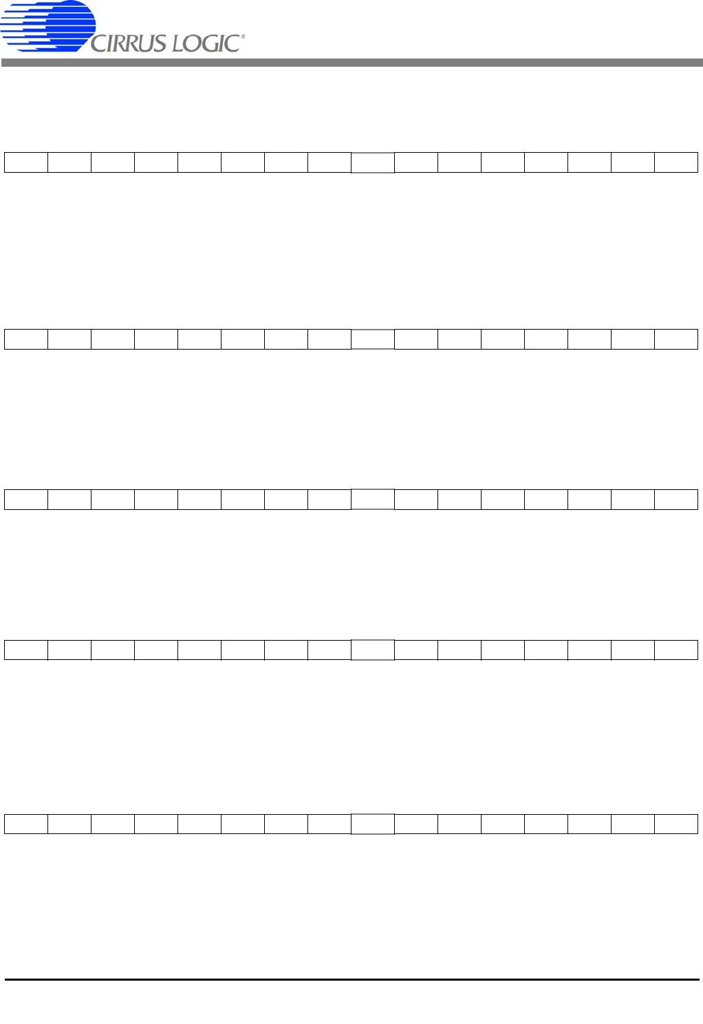
MSB LSB
-(2
0
)2
-1
2
-2
2
-3
2
-4
2
-5
2
-6
2
-7
.....
2
-17
2
-18
2
-19
2
-20
2
-21
2
-22
2
-23
MSB LSB
-(2
0
)2
-1
2
-2
2
-3
2
-4
2
-5
2
-6
2
-7
.....
2
-17
2
-18
2
-19
2
-20
2
-21
2
-22
2
-23
MSB LSB
-(2
0
)2
-1
2
-2
2
-3
2
-4
2
-5
2
-6
2
-7
.....
2
-17
2
-18
2
-19
2
-20
2
-21
2
-22
2
-23
MSB LSB
-(2
7
)2
6
2
5
2
4
2
3
2
2
2
1
2
0
.....
2
-10
2
-11
2
-12
2
-13
2
-14
2
-15
2
-16
MSB LSB
-(2
0
)2
-1
2
-2
2
-3
2
-4
2
-5
2
-6
2
-7
.....
2
-17
2
-18
2
-19
2
-20
2
-21
2
-22
2
-23