CS5464
DS682F3 37
8.3.13 Temperature Gain (T
GAIN
) Address: 22
Default = 0x2F02C3
Refer to 6.13
Temperature Measurement on page 21 for more information.
8.3.14 Temperature Offset (T
OFF
) Address: 23
Default = 0xF3D35A
Refer to 6.13
Temperature Measurement on page 21 for more information.
8.3.15 Filter Settling Time for Conversion Startup (T
SETTLE
) Address: 25
Default = 30
Sets the number of output word rate (OWR) samples that will be used to allow filters to settle at the beginning
of Conversion and Calibration commands. This is an integer in the range of 0 to 8,388,607 samples.
8.3.16 No Load Threshold (Load
MIN
) Address 26
Default = 0
Load
MIN
is used to set the no load threshold. When the magnitude of the E
PULSE
register is less than Load
MIN
,
E
PULSE
will be zeroed. If the magnitude of the Q
PULSE
register is less than Load
MIN
, Q
pulse
will be zeroed.
Load
MIN
is a two’s compliment value in the range of -1.0 value 1.0, with the binary point to the right of the
MSB. Negative values are not used.
8.3.17 Voltage Fixed RMS Reference (VF
RMS
) Address 27
Default = 0.7071068 (full scale RMS)
If the application program detects that the meter has possibly been tampered with in such a manner that the
voltage input is no longer working, it may choose to use this internal RMS reference instead of the disabled volt-
age input by setting the VFIX bit in the
Modes register. This is a two's complement value in the range of
0
value 1.0, with the binary point to the right of the MSB. Negative values are not used.
MSB LSB
2
6
2
5
2
4
2
3
2
2
2
1
2
0
2
-1
.....
2
-11
2
-12
2
-13
2
-14
2
-15
2
-16
2
-17
MSB LSB
-(2
0
)2
-1
2
-2
2
-3
2
-4
2
-5
2
-6
2
-7
.....
2
-17
2
-18
2
-19
2
-20
2
-21
2
-22
2
-23
MSB LSB
2
23
2
22
2
21
2
20
2
19
2
18
2
17
2
16
.....
2
6
2
5
2
4
2
3
2
2
2
1
2
0
MSB LSB
-(2
0
)2
-1
2
-2
2
-3
2
-4
2
-5
2
-6
2
-7
.....
2
-17
2
-18
2
-19
2
-20
2
-21
2
-22
2
-23
MSB LSB
-(2
0
)2
-1
2
-2
2
-3
2
-4
2
-5
2
-6
2
-7
.....
2
-17
2
-18
2
-19
2
-20
2
-21
2
-22
2
-23
CS5464
38 DS682F3
8.3.18 System Gain (G) Address: 28
Default = 1.25
System Gain (
G) is applied to all channels. By default, G = 1.25, but can be finely adjusted to compensate for
voltage reference error. It is a two's complement value in the range of -2.0
value 2.0, with the binary point to
the right of the second MSB. Values should be kept within 5% of 1.25.
8.3.19 System Time (Time) Address: 29
Default = 0
System Time (
Time) is measured in output word rate (OWR) samples. This is an unsigned integer in the range
of 0 to 16,777,215 samples. At 4.0 kHz, OWR it will overflow every 1 hour, 9 minutes, and 54 seconds.
Time
can be used by the application to manage real-time events.
8.4 Page 2 Registers
8.4.1 Voltage Sag and Current Fault Duration (V1Sag
DUR
, V2Sag
DUR ,
I1Fault
DUR ,
I2Fault
DUR
)
Address: 0 (V1Sag
DUR
), 8 (V2Sag
DUR
), 4 (I1Fault
DUR
), 12 (I2Fault
DUR
)
Default = 0
Voltage sag duration,
V1Sag
DUR
(V2Sag
DUR
) and current fault duration, I1Fault
DUR
(I2Fault
DUR
) determine the
count of output word rate (OWR) samples utilized to determine a sag or fault event. These are integers in the
range of 0 to 8,388,607 samples. A value of zero disables the feature.
8.4.2 Voltage Sag and Current Fault Level (V1Sag
LEVEL
, V2Sag
LEVEL
, I1Fault
LEVEL
, I2Fault
LEVEL
)
Address: 1 (V1Sag
LEVEL
), 9 (V2Sag
LEVEL
), 5 (I1Fault
LEVEL
), 13 (I2Fault
LEVEL
)
Default = 0
Voltage sag level,
V1Sag
LEVEL
(V2Sag
LEVEL
) and current fault level, I1Fault
LEVEL
(I2Fault
LEVEL
) establish an
input level below which a sag or fault is triggered These are two's complement values in the range of
-1.0
value 1.0, with the binary point to the right of the MSB. Negative values are not used.
MSB LSB
-(2
1
)2
0
2
-1
2
-2
2
-3
2
-4
2
-5
2
-6
.....
2
-16
2
-17
2
-18
2
-19
2
-20
2
-21
2
-22
MSB LSB
2
23
2
22
2
21
2
20
2
19
2
18
2
17
2
16
.....
2
6
2
5
2
4
2
3
2
2
2
1
2
0
MSB LSB
0
2
22
2
21
2
20
2
19
2
18
2
17
2
16
.....
2
6
2
5
2
4
2
3
2
2
2
1
2
0
MSB LSB
-(2
0
)2
-1
2
-2
2
-3
2
-4
2
-5
2
-6
2
-7
.....
2
-17
2
-18
2
-19
2
-20
2
-21
2
-22
2
-23
CS5464
DS682F3 39
9. SYSTEM CALIBRATION
9.1 Calibration
The CS5464 provides DC offset and gain calibration
that can be applied to the voltage and current measure-
ments, and AC offset calibration which can be applied to
the voltage and current RMS calculations.
Since the voltage and current channels have indepen-
dent offset and gain registers, offset and gain calibra-
tion can be performed on any channel independently.
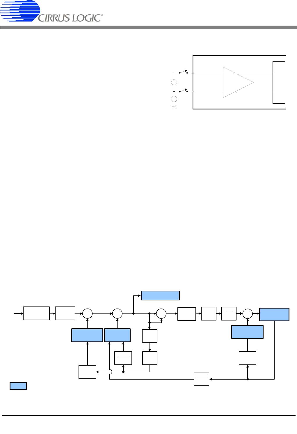
The data flow of the calibration is shown in Figure 10.
The CS5464 must be operating in its active state and
ready to accept valid commands. Refer to 7.6
Com-
mands
on page 24.
The value in the Cycle Count register (
N) determines
the number of output word rate (OWR) samples that are
averaged during a calibration. DC offset and gain cali-
brations take at least
N + T
SETTLE
samples. AC offset
calibrations take at least 6(
N)+T
SETTLE
samples. As N
is increased, the accuracy of calibration results tends to
also increase.
The DRDY bit in the
Status register will be set at the
completion of Calibration commands. If an overflow oc-
curs during calibration, other
Status register bits may be
set as well.
9.1.1 Offset Calibration
During offset calibrations, no line voltage or current
should be applied to the meter. A zero-volt differential
signal can also be applied to the voltage inputs VIN
or
current inputs IIN1
(IINof the CS5464.
(see Figure 11.)
9.1.1.1 DC Offset Calibration
The DC Offset Calibration command measures and av-
erages DC values read on specified voltage or current
channels at zero input and stores the inverse result in
the associated offset registers. This will be added to in-
stantaneous measurements in subsequent conver-
sions, removing the offset.
Gain registers for channels being calibrated should be
set to 1.0 prior to performing DC offset calibration.
9.1.1.2 AC Offset Calibration
The AC Offset Calibration command measures the re-
sidual RMS values read on specified voltage or current
channels at zero input and stores the inverse result in
the associated AC offset registers. This will be added to
RMS measurements in subsequent conversions, re-
moving the offset.
AC offset registers for channels being calibrated should
first be cleared prior to performing the calibration.
In
Modulator
+
X
V1, I1, V2, I2
Filter
N
I1
RMS
, V1
RMS
,
I2
RMS
, V2
RMS
I1
DCOFF
, V1
DCOFF
,
I2
DCOFF
, V2
DCOFF
I1
GAIN
, V1
GAIN
,
I2
GAIN
, V2
GAIN
0.6
+
= READABLE/WRITABLE REGISTERS.
N
+
X
N
1
DC
AVG
RMS
I1
ACOFF
, V1
ACOFF
,
I2
ACOFF
, V2
ACOFF
N
+
DC Gain
DC Offset
AC Offset
RMS
AC Gain
Negate
DC AVG
Negate
Figure 10. Calibration Data Flow
+
-
XGAIN
+
-
External
Connections
0V
+
-
AIN+
AIN-
CM
+
-
Figure 11. System Calibration of Offset

CS5464-IS

Mfr. #:
Manufacturer:
Cirrus Logic
Description:
Current & Power Monitors & Regulators 3-Ch Single Phase Power/Energy IC
Lifecycle:
New from this manufacturer.
Delivery:
DHL FedEx Ups TNT EMS
Payment:
T/T Paypal Visa MoneyGram Western Union

Products related to this Datasheet