CS5464
8 DS682F3
ANALOG CHARACTERISTICS (Continued)
Notes: 3. Applies before system calibration.
4. All outputs unloaded. All inputs CMOS level.
5. Measurement method for PSRR: VREFIN tied to VREFOUT, VA+ = VD+ = 5 V, a 150 mV
(zero-to-peak) (60 Hz) sinewave is imposed onto the +5 V DC supply voltage at VA+ and VD+ pins. The
“+” and “-” input pins of both input channels are shorted to AGND. The CS5464 is then commanded to
continuous conversion acquisition mode, and digital output data is collected for the channel under test.
The (zero-to-peak) value of the digital sinusoidal output signal is determined, and this value is converted
into the (zero-to-peak) value of the sinusoidal voltage (measured in mV) that would need to be applied
at the channel’s inputs, in order to cause the same digital sinusoidal output. This voltage is then defined
as Veq. PSRR is (in dB)
:
6. When voltage level on PFMON is sagging, and LSD bit = 0, the voltage at which LSD is set to 1.
7. If the LSD bit has been set to 1 (because PFMON voltage fell below PMLO), this is the voltage level on
PFMON at which the LSD bit can be permanently reset back to 0.
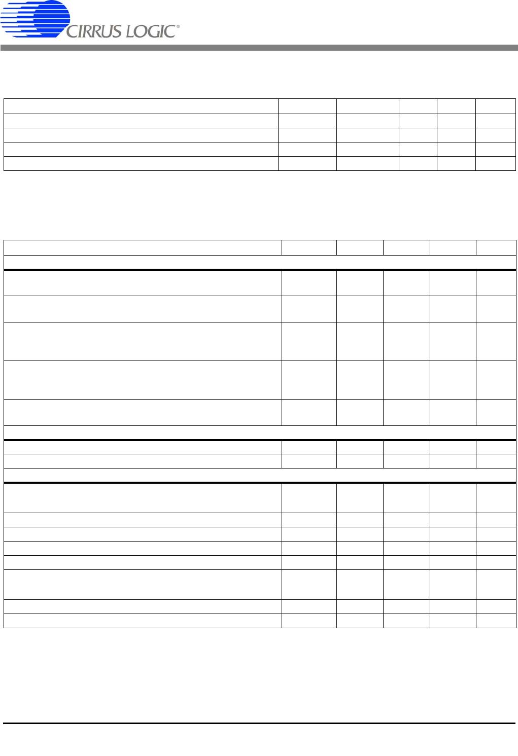
Parameter Symbol Min Typ Max Unit
Analog Inputs (Voltage Inputs)
Differential Input Range
[(VIN+) – (VIN-)] VIN - 500 - mV
P-P
Total Harmonic Distortion THD 65 75 - dB
Crosstalk from Current Inputs at Full Scale
(50, 60 Hz) --70-dB
Input Capacitance
All Gain Ranges IC - 2.0 - pF
Effective Input Impedance EII 2 - - M
Noise (Referred to Input) N
V
--140µV
rms
Offset Drift (Without the High-pass Filter) OD - 16.0 - µV/°C
Gain Error
(Note 3) GE - ±3.0 %
Temperature
Temperature Accuracy T - ±5 - °C
Power Supplies
Power Supply Currents (Active State)
I
A+
I
D+
(VA+ = VD+ = 5 V)
I
D+
(VA+ = 5 V, VD+ = 3.3 V)
PSCA
PSCD
PSCD
-
-
-
1.5
3.5
2.3
-
-
-
mA
mA
mA
Power Consumption
Active State (VA+ = VD+ = 5 V)
(Note 4) Active State (VA+ = 5 V, VD+ = 3.3 V)
Stand-by State
Sleep State
PC
-
-
-
-
25
15
7
10
33
20
-
-
mW
mW
mW
uW
Power Supply Rejection Ratio
(50, 60 Hz)
(Note 5)
Voltage
Current
(Gain = 50x)
Current (Gain = 10x)
PSRR
48
68
60
55
75
65
-
-
-
dB
dB
dB
PFMON Low-voltage Trigger Threshold
(Note 6) PMLO 2.3 2.45 - V
PFMON High-voltage Power-on Trip Point
(Note 7) PMHI - 2.55 2.7 V
PSRR 20
150
V
eq
--------- -
log=