CS5464
DS682F3 31
8.2.12 Internal Status (Status) and Interrupt Mask (Mask)
Address: 15 (Status); 26 (Mask)
Default = 1 (
Status), 0 (Mask)
The
Status register indicates a variety of conditions within the chip. Writing a '1' to a Status register bit will clear
that bit if the condition that set it has been removed. Writing a '0' to any bit has no effect.
The
Mask register is used to control the activation of the INT pin. Placing a logic '1' to a Mask register bit will
allow the corresponding
Status register bit to activate the INT pin when set.
DRDY Data Ready. During conversion, this bit indicates that low-rate results have been updated.
It indicates completion of other commands and the reset sequence.
I1OR (I2OR) Current Out of Range. Set when the measured current would cause the
I1 (I2) register to
overflow.
V1OR (V2OR) Voltage Out of Range. Set when the measured voltage would cause the
V1 (V2) register to
overflow.
CRDY Conversion Ready. Indicates that sample rate (output word rate) results have been updat-
ed.
I1ROR (I2ROR) RMS Current Out of Range. Set when RMS current would cause the
I1
RMS
(I2
RMS
) register
to overflow.
V1ROR (V2ROR) RMS Voltage Out of Range. Set when RMS voltage would cause the
V1
RMS
(V2
RMS
) reg-
ister to overflow.
E1OR (E2OR) Energy Out of Range. Set when average power would cause
P1
AVG
(P2
AVG
) to overflow.
I1FAULT (I2FAULT)Indicates when a current fault condition has occurred.
V1SAG (V2SAG) Indicates when a voltage sag condition has occurred.
TUP Indicates when the Temperature register (
T) has been updated.
TOD Modulator oscillation has been detected in the temperature A/D.
VOD Modulator oscillation has been detected in the voltage A/D.
I1OD (I2OD) Modulator oscillation has been detected in the current1 (current2) A/D.
LSD Low Supply Detect. Set when the voltage on the PFMON pin falls below the specified low
level. LSD bit cannot be reset until the voltage rises above the specified high level.
FUP Frequency Updated. Indicates the
Epsilon register has been updated.
IC
Invalid Command. Normally logic 1. Set to 0 when an invalid command is received. It may
also indicate loss of serial command synchronization and the part may need to be re-initial-
ized.
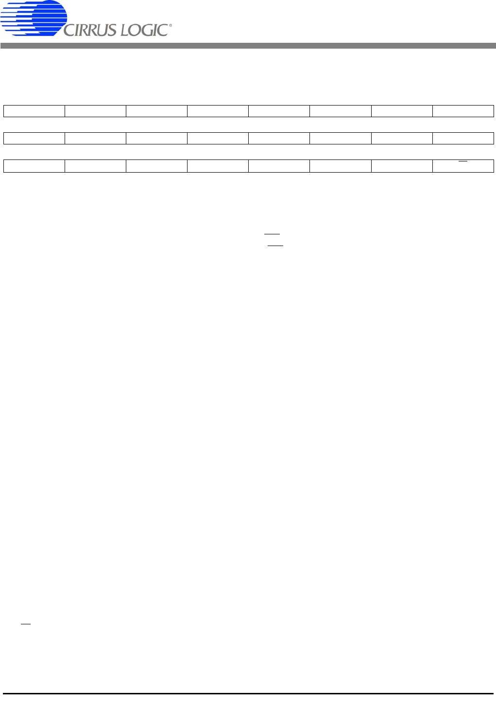
23 22 21 20 19 18 17 16
DRDY I2OR V2OR CRDY I2ROR V2ROR I1OR V1OR
15 14 13 12 11 10 9 8
E2OR I1ROR V1ROR E1OR I1FAULT V1SAG I2FAULT V2SAG
76543210
TUP TOD I2OD VOD I1OD LSD FUP
IC